Table 7-15, Memory (ddr) interface signals – AMD Geode LX [email protected] User Manual
Page 614
614
AMD Geode™ LX Processors Data Book
Electrical Specifications
33234H
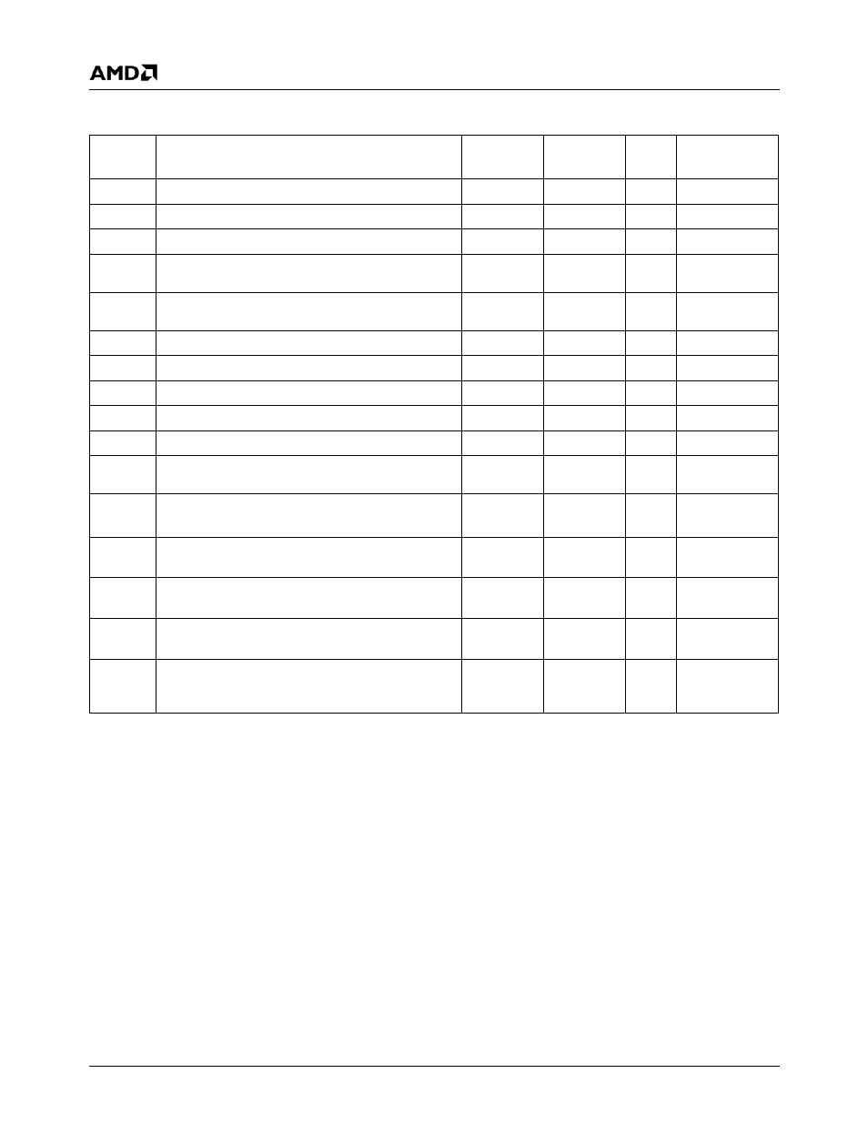
Table 7-15. Memory (DDR) Interface Signals
Symbol
(Note 1)
Parameter
Min
Max
Unit
Comments
t
CK
SDCLK[5:0]P, SDCLK[5:0]N period
5.0
ns
Note 2
t
CH
SDCLK[5:0]P, SDCLK[5:0]N High time
2.4
ns
48% t
CK
t
CL
SDCLK[5:0]P, SDCLK[5:0]N Low time
2.4
ns
48% t
CK
t
SKEW1
SDCLK[n]P to SDCLK[n]N skew (n=0..5)
0.1
ns
Guaranteed by
design
t
DEL1
SDCLK[5:1]P, SDCLK[5:0]N edge delay from
SDCLK[0]P
-0.2
0.2
ns
Note 2, Note 3
DQS[7:0] Input and output period
5.0
ns
Same as t
CK
t
DQSCK
DQS[7:0] Input delay relative to SDCLK[5:0]
-0.5
t
CK
-2 ns
Note
4
t
DEL2
DQS[7:0] output edge delay from SDCLK[5:0]
-0.5
0.5
ns
t
RPRE
DQS input preamble before first DQS rising edge
0.25*t
CK
ns
t
RPST
DQS input postamble after last DQS rising edge
0.25*t
CK
t
WPRE
DQS output write preamble valid time before
SDCLK[5:0] rising edge
0.5*t
CK
-0.4
0.5*t
CK
+1
ns
t
WPST
DQS output write postamble after last DQS falling
edge
0.75*t
CK
-0.4
0.75*t
CK
+1
ns
t
DQSQs
DQ[63:0] Input setup time from DQS
-0.25*t
CK
+0.5
ns
t
DQSQh
DQ[63:0] Input hold time from DQS
0.25*t
CK
+0.5
ns
t
VAL1
DQ[63:0], DQM[7:0] Output Data Valid Delay time
from DQS rising OR falling edge
0.25*t
CK
-0.4
0.25*t
CK
+0.4
ns
t
VAL2
MA[12:0], BA[1:0], CAS[1:0]#, RAS[1:0]#,
CKE[1:0], CS[3:0]#, WE[1:0] Output Valid Delay
time from SDCLK[5:0]
1.1
3.0
ns
Note 1. Refer to Figure 7-8 "DDR Write Timing Measurement Points" on page 615 and Figure 7-9 "DDR Read Timing Mea-
Note 2. The SDCLKP and SDCLKN clocks are inversions of each other (differential clocking).
Note 3. These parameters guarantee device timing, but they may be tested to a looser value to allow for tester uncertain-
ties. Devices that meet the loosened tester values meet specs when correlated with lab measurements.
Note 4. t
VAL2
and t
DQSCK
timings are achieved for different DIMM loadings by proper initial settings of the
GLCP_DELAY_CONTROLS MSR. Typical tester results with clock and address loaded equally and no pro-
grammed delay for address are 0 ns for t
VAL2
.
Note 5. The DQ timing relative to DQS are on a per-byte basis only. DQ[7:0] and DQM[0] should be measured against
DQS[0], DQ[15:8] and DQM[1] should be measured against DQS[1], etc.