Figure 7-3, Table 7-8, System interface signals – AMD Geode LX [email protected] User Manual
Page 608
608
AMD Geode™ LX Processors Data Book
Electrical Specifications
33234H
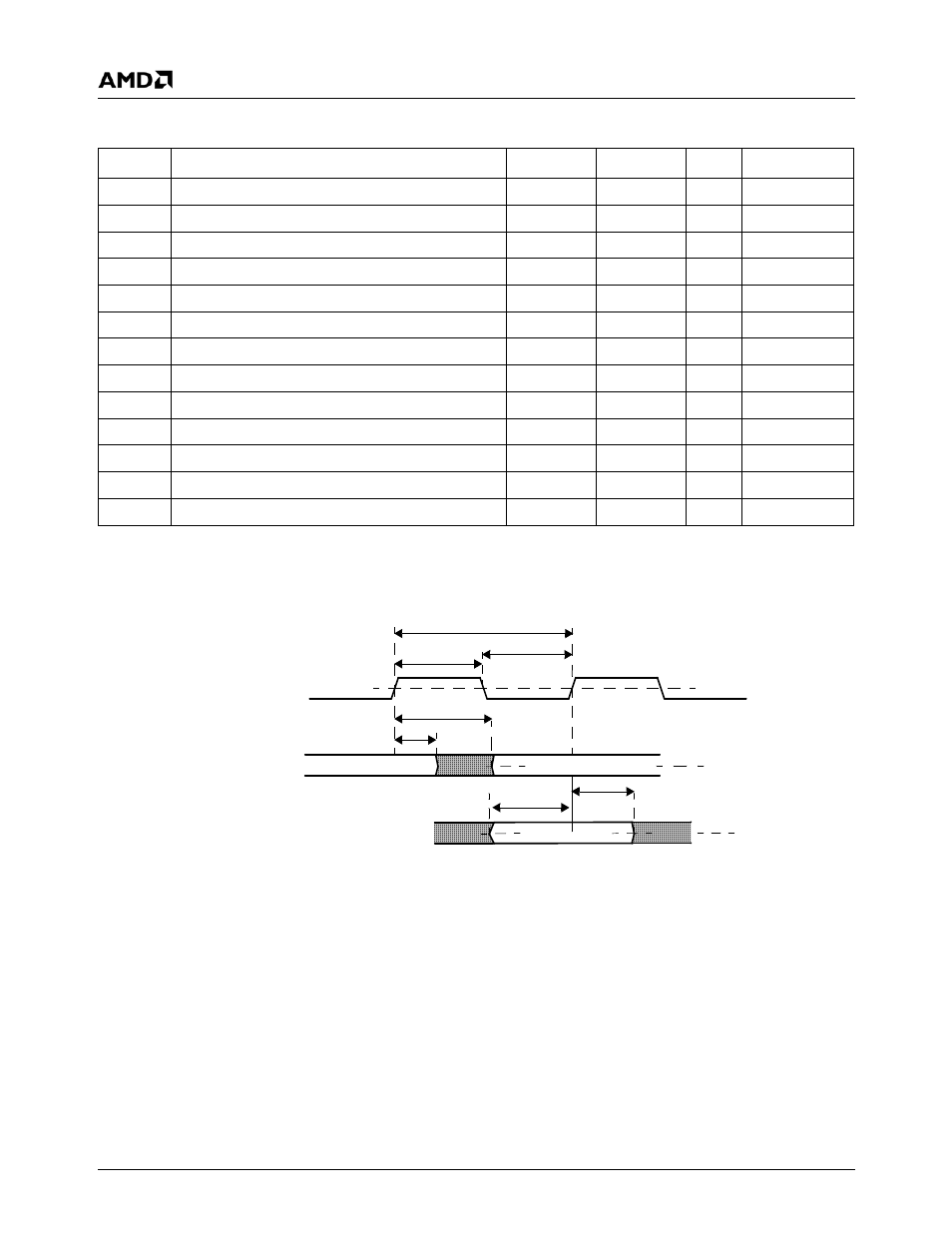
Figure 7-3. Drive Level and Measurement Points for Switching Characteristics
Table 7-8. System Interface Signals
Symbol
Parameter
Min
Max
Unit
Comments
t
CK
SYSREF Cycle time
15.0
INF
ns
66 MHz
t
CH
SYSREF High time
6.0
ns
40% t
CK
t
CL
SYSREF Low time
6.0
ns
40% t
CK
t
SU1
RESET# Setup time to SYSREF
3
ns
Note 1
t
H1
RESET# Hold time from SYSREF
1
ns
Note 1
t
SU2
CIS Setup time to SYSREF
3.0
ns
t
H2
CIS Hold time from SYSREF
0
ns
t
VAL1
IRQ13 Valid Delay time from SYSREF
2.0
6.0
ns
t
VAL2
SUSPA# Valid Delay time from SYSREF
2.0
6.0
ns
t
ON
V
IO
and V
MEM
power on after V
CORE
0
100
ms
Note 2
t
MVON
MVREF power on after V
MEM
0
100
ms
t
RSTX
Reset Active time after SYSREF clock stable
100
us
For PLL lock
t
Z
Output drive delay after RESET# released
20
ns
Note 1. RESET# is asynchronous. The setup/hold times stated are for testing purposes that require sequential repeatabil-
ity.
Note 2. For proper powerup of DRGB and flat panel controls, V
IO
must power up after V
CORE
. Otherwise, V
CORE
can be
last.
SYSREF
Outputs
Inputs
50%
Valid Input
Valid Output
n+1
Valid Output
n
50%
50%
t
VAL1,2
Min
t
VAL1,2
Max
t
SU1,2
t
H1,2
t
CK
t
CH
t
CL