5 display controller, Display controller, Figure 6-12 – AMD Geode LX [email protected] User Manual
Page 278: Display controller high-level block diagram
278
AMD Geode™ LX Processors Data Book
Display Controller
33234H
6.5
Display Controller
The Display Controller (DC) module retrieves graphics,
video, and overlay streams from the frame buffer, serial-
izes the streams, performs any necessary color lookups
and output formatting, and interfaces to the VP for driving
the display device.
Features
• 512x64-bit display FIFO
• 64x64x2-bit hardware cursor
• 64x vertical resolution x2-bit hardware icon overlay
• 3x261x8-bit palette/gamma RAM (including five exten-
sion colors)
• Display refresh compression
• 64x64-bit compressed line buffer
• Flexible timing generator
• Support for Video Blanking Interval (VBI) data
• Support for interlaced modes up to 1920x1080
• 3-tap flicker filter for support of interlaced NTSC and
PAL display modes
• Flexible memory addressing
• Video overlay support
• Independent VGA block for complete hardware VGA
implementation
• Dirty/Valid RAM and controller to monitor memory traffic
in support of display refresh compression
• Six 512x64-bit line buffers to support downscaling and
flicker filtering
• 3x5-tap graphics filter for scaling and filtering
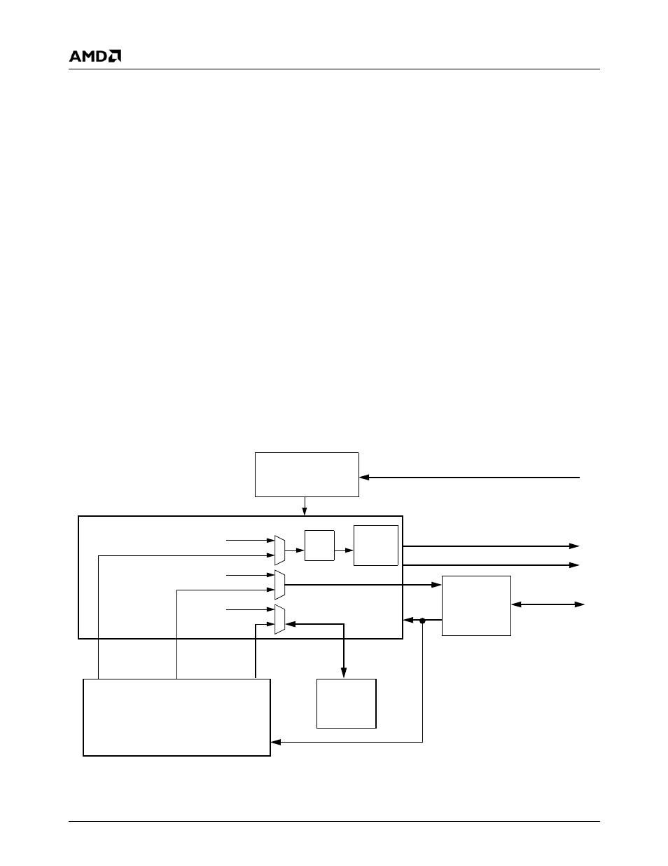
The DC module consists of a GUI (Graphical User Inter-
face) block, a VGA block, and back-end scaling/filter. The
GUI is compatible with the Display Controller found in the
GX processor. The VGA block provides hardware compati-
bility with the VGA graphics standard. The GUI and VGA
blocks share a single display FIFO and display refresh
memory interface to the memory controller. The VGA block
passes 8-bpp and syncs to the GUI, which expands the
pixels to 24-bpp via the CLUT (color lookup table). The
VGA block also passes the information to the graphics filter
for scaling and interlaced display support. This stream is
then passed to the Video Processor (VP), which is used for
video overlay. The VP forwards this information to the DAC
(Digital-to-Analog Converter), which generates the analog
red, green, and blue signals and buffers the sync signals,
that are then sent to the display. The VP output can also be
rendered as YUV data that can be output on the Video Out-
put Port. The DC block diagram is shown in Figure 6-12.
Figure 6-12. Display Controller High-Level Block Diagram
VGA Block
Graphical User Interface Block
FIFO
Host I/F
FIFO
Pixel, Syncs, DISPEN
Display Memory I/F
Display Refresh
Memory Control
8-Bit Pixel,
Syncs,
Display enable
CTL
Dirty/Valid Flags
Video Data Output to VP
Dirty/Valid RAM
and Control
GLIU0 Port
GLIU0 Memory Port
GeodeLink™
Interface
Unit 0
(GLIU0)
CLUT
Graphics
Scaler/
Filter