19 glcp throttle or c2 start delay (glcp_th_sd), 20 glcp scale factor (glcp_th_sf), Glcp throttle or c2 start delay (glcp_th_sd) – AMD Geode LX [email protected] User Manual
Page 561: Glcp scale factor (glcp_th_sf), 00000000_00000000h
AMD Geode™ LX Processors Data Book
561
GeodeLink™ Control Processor Register Descriptions
33234H
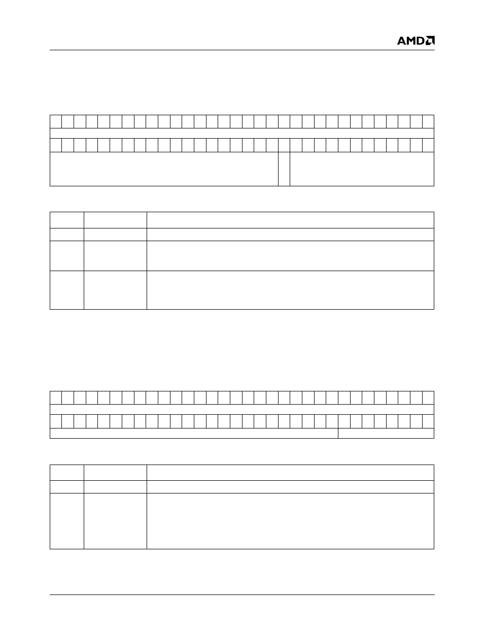
6.14.2.19 GLCP Throttle or C2 Start Delay (GLCP_TH_SD)
6.14.2.20 GLCP Scale Factor (GLCP_TH_SF)
MSR Address
4C00001Ch
Type
R/W - I/O Offset 10h
Reset Value
00000000_00000000h
GLCP_TH_SD Register Map
63 62 61 60 59 58 57 56 55 54 53 52 51 50 49 48 47 46 45 44 43 42 41 40 39 38 37 36 35 34 33 32
RSVD
31 30 29 28 27 26 25 24 23 22 21 20 19 18 17 16 15 14 13 12 11 10
9
8
7
6
5
4
3
2
1
0
RSVD
P_L
V
L2_IN
THT_DELAY
GLCP_TH_SD Bit Descriptions
Bit
Name
Description
63:13
RSVD
Reserved. By convention, always write zero.
12
P_LVL2_IN
Enable Indicator. If P_LVL2 (in MSR 4C000019h) was read, then this bit reads high. If
this bit is written to a one, the suspend is aborted. This bit is always cleared and Suspend
de-asserted on NMI, IRQ, SSMI, ASMI, DMI, or system Sleep.
11:0
THT_DELAY
Throttle Delay. Indicates how long to wait before beginning the processor throttling pro-
cess as defined by MSR 4C000018h. The delay setting is multiplied by 16 to get the
number of PCI clock cycles to wait, thus setting THT_DELAY = 3 causes a wait of 48 PCI
clock cycles.
MSR Address
4C00001Dh
Type
R/W - I/O Offset 14h
Reset Value
00000000_00000000h
GLCP_TH_SF Register Map
63 62 61 60 59 58 57 56 55 54 53 52 51 50 49 48 47 46 45 44 43 42 41 40 39 38 37 36 35 34 33 32
RSVD
31 30 29 28 27 26 25 24 23 22 21 20 19 18 17 16 15 14 13 12 11 10
9
8
7
6
5
4
3
2
1
0
RSVD
SCALE
GLCP_TH_SF Bit Descriptions
Bit
Name
Description
63:8
RSVD
Reserved. By convention, always write 0.
7:0
SCALE
Scale Factor. This value is used in conjunction with CLK_VAL in the GLCP_CNT MSR
(4C000018h[3:0]). This value times CLK_VAL (or 15-CLK_VAL) indicates the number of
PCI clock cycles to wait during processor active (or suspend) periods. The setting is mul-
tiplied by 16 to get the number of PCI clock cycles per period, thus SCALE = 3 and
CLK_VAL = 5 will have the processor active for 240 PCI clocks and suspended for 480
PCI clocks.