4 graphics processor register definitions, Graphics processor register definitions, Table 6-28 – AMD Geode LX [email protected] User Manual
Page 254: Standard geodelink™ device msrs summary, Table 6-29, Graphics processor configuration register summary
254
AMD Geode™ LX Processors Data Book
Graphics Processor Register Definitions
33234H
6.4
Graphics Processor Register Definitions
The registers associated with the Graphics Processor (GP)
are the Standard GeodeLink™ Device (GLD) MSRs and
Graphics Processor Configuration registers. Table 6-28
and Table 6-29 are register summary tables that include
reset values and page references where the bit descrip-
tions are provided.
The Standard GLD MSRs (accessed via the RDMSR and
WRMSR instructions) control the Graphics Processor’s
behavior as a GLIU module. These registers should be
programmed at configuration time and left alone thereafter.
They do not need to be modified by software to set up any
of the graphics primitives. The MSRs are 64 bits wide,
although not all bits are used in each register. Unused bits
marked as “write as read” return the value that was last
written to them. All other unused bits return 0.
All of the GP registers are accessible by the CPU through
memory mapped reads and writes on the GLIU. Note that
due to the pipelining operation of the GP, the value
returned during a read is the value stored in the slave reg-
ister, while the value in the master register is the actual
value being used by an ongoing BLT or vector operation.
Also note that the command buffer has the ability to write
into the slave registers. There is no reason, therefore, to
read registers other than the GP_BLT_STATUS,
GP_INT_CNTRL, and command buffer registers while the
command buffer is active.
Reserved bits, marked as “write as read,” indicate that
there is a real register backing those bits, which may be
used in some future implementation of the GP. Reserved
register bits that do not have a register backing them
always return a 0, regardless of what value software
decides to write into them.
The GP register space occupies 4 KB of the memory map.
The bottom 256 bytes are defined as access to GP’s pri-
mary registers. The remainder of the lower 1K of address
space is used to alias the host source register for the
source channel, allowing REP MOVS access. The upper
3K of address space is used to alias the host source regis-
ter for channel 3. This is the only aliasing that is supported
by the GP, so all register accesses should use the full 12-
bit offset.
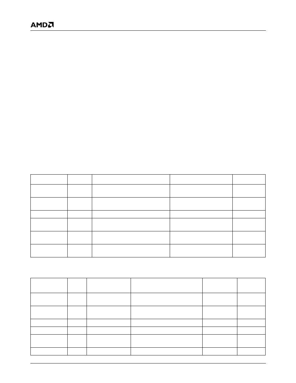
Table 6-28. Standard GeodeLink™ Device MSRs Summary
MSR Address
Type
Register Name
Reset Value
Reference
A0002000h
RO
GLD Capabilities MSR
(GLD_MSR_CAP)
00000000_0003D4xxh
A0002001h
R/W
GLD Master Configuration MSR
(GLD_MSR_CONFIG)
00000000_00000000h
A0002002h
R/W
00000000_00000000h
A0002003h
R/W
00000000_00000000h
A0002004h
R/W
GLD Power Management MSR
(GLD_MSR_PM)
00000000_00000000h
A0002005h
R/W
GLD Diagnostic MSR
(GLD_MSR_DIAG)
00000000_00000000h
Table 6-29. Graphics Processor Configuration Register Summary
GP Memory
Offset
Type
Group
Register Name
Reset Value
Reference
00h
R/W
Address Config
Destination Offset
(GP_DST_OFFSET)
00000000h
04h
R/W
Address Config
00000000h
R/W
Vector Config
00000000h
08h
R/W
Address Config
00000000h
0Ch
R/W
BLT Config
BLT Width/Height
(GP_WID_HEIGHT)
00000000h
Vector Config
00000000h