Figure 6-5, Loi addressing example, Figure 6-6 – AMD Geode LX [email protected] User Manual
Page 212: Loi example
212
AMD Geode™ LX Processors Data Book
GeodeLink™ Memory Controller
33234H
Auto Low Order Interleaving
The GLMC requires that module banks [0:1], if both
installed, be identical and module banks [2:3], if both
installed, be identical. Standard DIMMs and SODIMMs are
configured this way. Because of this requirement, when
module banks [0:1] are installed or module banks [2:3] are
installed, LOI is in effect, when enabled for those bank
pairs. If all four module banks [0:3] are identical, then LOI
is in effect across all four module banks.
LOI uses the least significant bits after the page bits to
select which bank the page is located in. An example is
shown in Figure 6-5.
As stated previously, for LOI to be most effective, module
banks [0:1] and module banks [2:3] must be of identical
configuration. LOI is least effective when only two module
banks are installed and of different configuration. This can
only happen when one of the module banks is installed in
module bank [0 or 1] and the second module bank is
installed in module bank [2 or 3]. LOI has the advantage of
creating an effective larger moving page throughout mem-
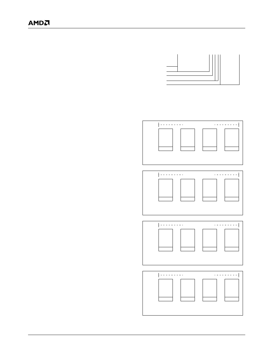
ory. Using an example of four identical module banks, with
four component banks, and a 1 KB address (8 KB data)
page, there would be an effective moving page of 64 KB of
data (see Figure 6-6).
Physical Address to DRAM Address Conversion
Tables 6-1 and 6-2 on page 213 show Auto LOI address
conversion examples when two DIMMs of the same size
are used in a system. Table 6-1 shows a one DIMM bank
conversion example, while Table 6-2 shows a two DIMM
bank example.
Tables 6-3 and 6-4 on page 214 show Non-Auto LOI
address conversion examples when either one or two
DIMMs of different sizes are used in a system. Table 6-3
shows a one DIMM bank address conversion example,
while Table 6-4 shows a two DIMM bank example. The
addresses are computed on a per DIMM basis.
Since the DRAM interface is 64 bits wide, the lower three
bits of the physical address get mapped onto the DQM[7:0]
lines. Thus, the address conversion tables (Tables 6-1
through 6-4) show the physical address starting from A3.
Figure 6-5. LOI Addressing Example
Figure 6-6. LOI Example
aaaaaaaaaaaaaaaaaaaaaaaaaa
22222222211111111110000000
87654321098765432109876543
RA[12:0]
MB[0]
BA[1:0]
CA[7:0]
MB[1]
Internal
Physical
Address
CA are the CAS addresses on MA[7:0]
RA are the RAS addresses on MA[12:0]
Module
Bank
0
Page 0
00000000h
00002000h
00004000h
00006000h
Component Banks
Page 0
Address
Page 0
Address
Page 0
Address
Page 0
Address
Bank
1
Page 0
Bank
2
Page 0
Bank 0
Bank
3
Page 0
Module
Bank
0
Page 0
00008000h
0000A000h
0000C000h
0000E000h
Component Banks
Page 0
Address
Page 0
Address
Page 0
Address
Page 0
Address
Bank
1
Page 0
Bank
2
Page 0
Bank 1
Bank
3
Page 0
Module
Bank
0
Page 0
00010000h
00012000h
00014000h
00016000h
Component Banks
Page 0
Address
Page 0
Address
Page 0
Address
Page 0
Address
Bank
1
Page 0
Bank
2
Page 0
Bank 2
Bank
3
Page 0
Module
Bank
0
Page 0
00018000h
0001A000h
0001C000h
0001E000h
Component Banks
Page 0
Address
Page 0
Address
Page 0
Address
Page 0
Address
Bank
1
Page 0
Bank
2
Page 0
Bank 3
Bank
3
Page 0