Geodelink™ memory controller register descriptions, Table 6-5, Standard geodelink™ device msrs summary – AMD Geode LX [email protected] User Manual
Page 219: Table 6-6, Glmc specific msr summary
AMD Geode™ LX Processors Data Book
219
GeodeLink™ Memory Controller Register Descriptions
33234H
6.2
GeodeLink™ Memory Controller Register Descriptions
All GLMC registers are Model Specific Registers (MSRs)
and are accessed via the RDMSR and WRMSR instruc-
tions.
The registers associated with the GLMC are the Standard
GeodeLink Device (GLD) MSRs and GLMC Specific
MSRs. Table 6-5 and Table 6-6 are register summary
tables that include reset values and page references where
the bit descriptions are provided.
Note:
MSR addresses are documented using the CPU
Core as the source. Refer to Section 4.1 "MSR
Set" on page 45 for further details.
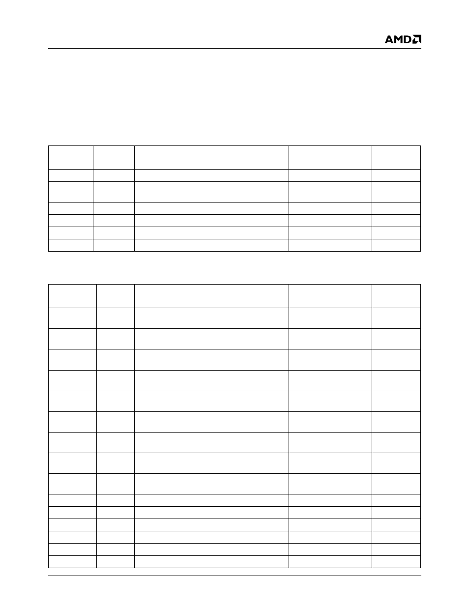
Table 6-5. Standard GeodeLink™ Device MSRs Summary
MSR
Address
Type
Register Name
Reset Value
Reference
20002000h
RO
GLD Capabilities MSR (GLD_MSR_CAP)
00000000_000204xxh
20002001h
---
GLD Master Configuration MSR
(GLD_MSR_CONFIG) - Not Used
00000000_00000000h
Page 220
20002002h
R/W
00000000_00000000h
20002003h
R/W
00000000_00000000h
20002004h
GLD Power Management (GLD_MSR_PM)
00000000_00000000h
20002005h
R/W
00000000_00000000h
Table 6-6. GLMC Specific MSR Summary
MSR
Address
Type
Register Name
Reset Value
Reference
20000010h
RO
Row Addresses Bank0 DIMM0, Bank1 DIMM0
(MC_CF_BANK01)
xxxxxxxx_xxxxxxxxh
20000011h
RO
Row Addresses Bank2 DIMM0, Bank3 DIMM0
(MC_CF_BANK23)
xxxxxxxx_xxxxxxxxh
20000012h
RO
Row Addresses Bank4 DIMM0, Bank5 DIMM0
(MC_CF_BANK45)
xxxxxxxx_xxxxxxxxh
20000013h
RO
Row Addresses Bank6 DIMM0, Bank7 DIMM0
(MC_CF_BANK67)
xxxxxxxx_xxxxxxxxh
20000014h
RO
Row Addresses Bank0 DIMM1, Bank1 DIMM0
(MC_CF_BANK89)
xxxxxxxx_xxxxxxxxh
20000015h
RO
Row Addresses Bank2 DIMM1, Bank3 DIMM1
(MC_CF_BANKAB)
xxxxxxxx_xxxxxxxxh
20000016h
RO
Row Addresses Bank4 DIMM1, Bank5 DIMM1
(MC_CF_BANKCD)
xxxxxxxx_xxxxxxxxh
20000017
RO
Row Addresses Bank6 DIMM1, Bank7 DIMM1
(MC_CF_BANKEF)
xxxxxxxx_xxxxxxxxh
20000018h
R/W
Refresh and SDRAM Program
(MC_CF07_DATA)
10071007_00000040h
20000019h
R/W
Timing and Mode Program (MC_CF8F_DATA)
18000008_287337A3h
2000001Ah
R/W
Feature Enables (MC_CF1017_DATA)
00000000_11080001h
2000001Bh
RO
Performance Counters (MC_CFPERF_CNT1)
00000000_00000000h
2000001Ch
R/W
Counter and CAS Control (MC_PERCNT2)
00000000_00FF00FFh
2000001Dh
R/W
Clocking and Debug (MC_CFCLK_DBUG)
00000000_00001300h
2000001Eh
RO
Page Open Status (MC_CFPG_OPEN)
00000000_0000FFFFh