0dch, Xxxxxxxxh, 0e0h – AMD Geode LX [email protected] User Manual
Page 352
352
AMD Geode™ LX Processors Data Book
Display Controller Register Descriptions
33234H
6.6.14.2 DC Even Field Video U Start Address Offset (DC_VID_EVEN_U_ST_OFFSET)
Settings written to this register do not take effect until the start of the next even interlaced field.
6.6.14.3 DC Even Field Video V Start Address Offset (DC_VID_EVEN_V_ST_OFFSET)
Settings written to this register do not take effect until the start of the next even interlaced field.
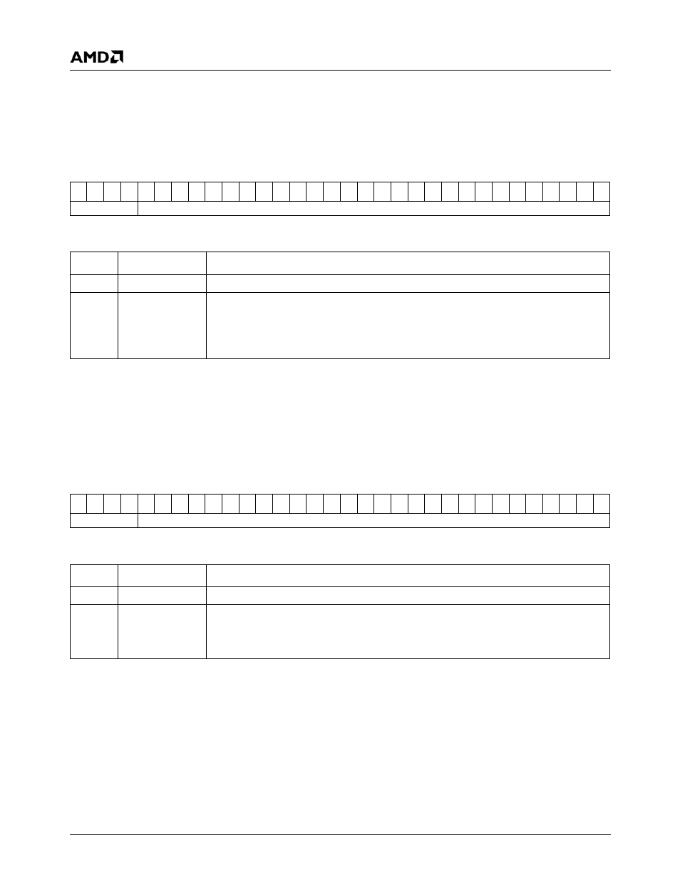
DC Memory Offset 0DCh
Type
R/W
Reset Value
xxxxxxxxh
DC_VID_EVEN_U_ST_OFFSET Register Map
31 30 29 28 27 26 25 24 23 22 21 20 19 18 17 16 15 14 13 12 11 10
9
8
7
6
5
4
3
2
1
0
RSVD
OFFSET
DC_VID_EVEN_U_ST_OFFSET Bit Descriptions
Bit
Name
Description
31:28
RSVD
Reserved. Set to 0.
27:0
OFFSET
Video U Even Buffer Start Offset. This value represents the starting location for Video
U Buffer for even fields when interlacing is enabled (DC Memory Offset 094h[11] = 1)
and YUV 4:2:0 mode is selected (DC Memory Offset 004h[20] = 1). The lower five bits
should always be programmed as zero so that the start offset is aligned to a 32-byte
boundary.
DC Memory Offset 0E0h
Type
R/W
Reset Value
xxxxxxxxh
DC_VID_EVEN_V_ST_OFFSET Register Map
31 30 29 28 27 26 25 24 23 22 21 20 19 18 17 16 15 14 13 12 11 10
9
8
7
6
5
4
3
2
1
0
RSVD
OFFSET
DC_VID_EVEN_V_ST_OFFSET Bit Descriptions
Bit
Name
Description
31:28
RSVD
Reserved. Set to 0.
27:0
OFFSET
Video V Even Buffer Start Offset. This value represents the starting location for Video
V Buffer for even fields when interlacing is enabled (DC Memory Offset 094h[11] = 1) and
YUV 4:2:0 is selected (DC Memory Offset 004h[20] = 1). The lower five bits should
always be programmed as zero so that the start offset is aligned to a 32-byte boundary.