Table 6-15, Rtm spi address/command register, Table 6-16 – Artesyn ATCA-7470 Installation and Use (October 2014) User Manual
Page 156: Rtm spi write register, Table 6-17, Rtm spi read register, Maps and registers
Maps and Registers
ATCA-7470 Installation and Use (6806800P15K)
156
A write access to the RTM SPI Address/Command Register starts the SPI transaction. The write
cycle terminates, when SPI transaction is finished.
A write access to the RTM SPI Address/Command Register with the Command Bit 0 (Write)
starts an SPI write transaction. The data byte is written to the SPI device.
A write access to the RTM SPI Address/Command Register with the Command Bit 1 (Read)
starts an SPI read transaction. This contains the data read from the SPI device.
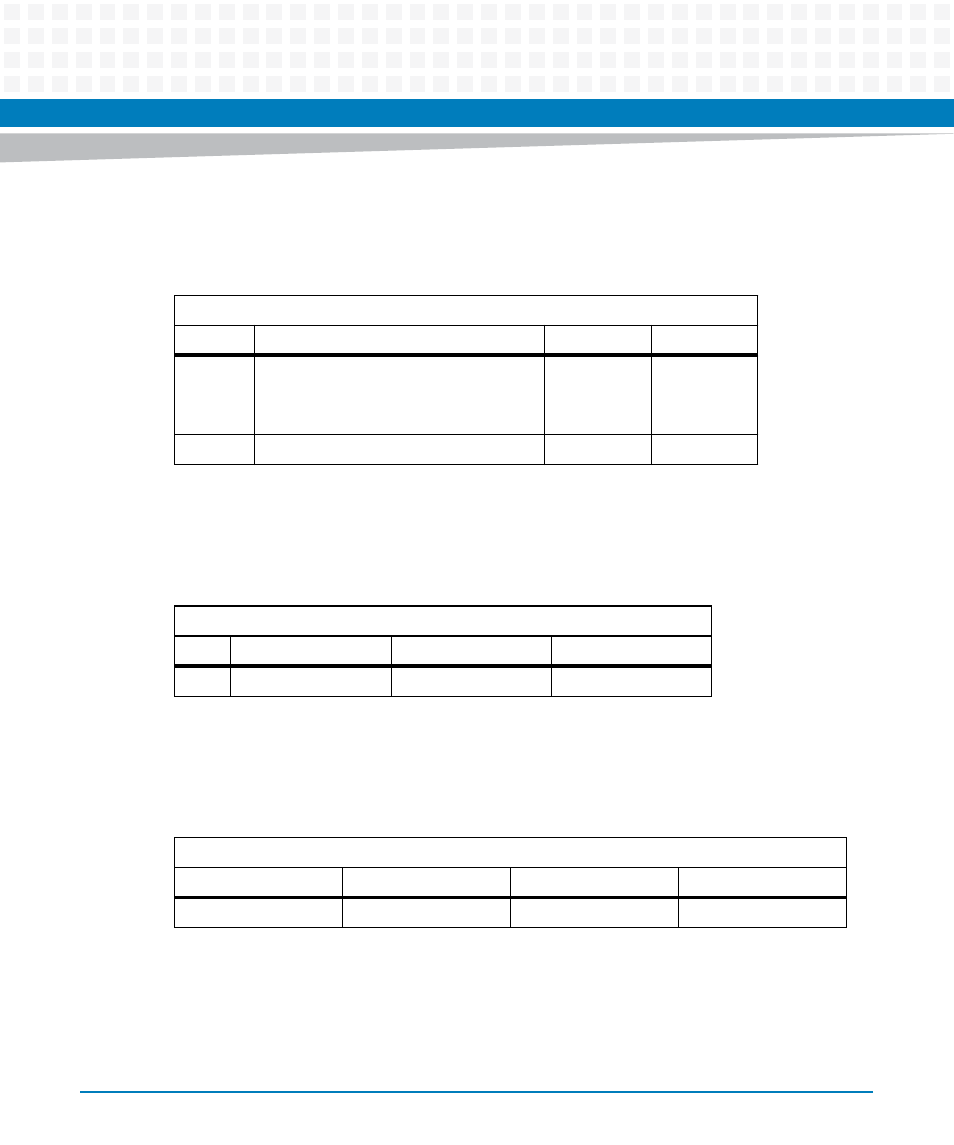
Table 6-15 RTM SPI Address/Command Register
Address Offset: 0x08
Bit
Description
Default
Access
0
Command Bit
0: Write
1: Read
0
LPC: r/w
7:1
RTM SPI Address bits [6:0]
0
LPC: r/w
Table 6-16 RTM SPI Write Register
Address Offset: 0x09
Bit
Description
Default
Access
7:0
RTM SPI write data
-
LPC: w
Table 6-17 RTM SPI Read Register
Address Offset: 0x09
Bit
Description
Default
Access
7:0
RTM SPI read data
0
LPC: r