2 spi register decoding, 2 post code register, Table 6-6 – Artesyn ATCA-7470 Installation and Use (October 2014) User Manual
Page 148: Lpc i/o register map overview, Table 6-7, Ipmc spi register, Maps and registers, Lpc i/o decoding
Maps and Registers
ATCA-7470 Installation and Use (6806800P15K)
148
6.3.1.1.1
LPC I/O Decoding
The LPC interface responds to LPC I/O accesses listed in the following table. All other LPC I/O
accesses are ignored.
All LPC I/O accesses to address POSTCODE and the address range REGISTERS are decoded by
the LPC core.
6.3.1.1.2 LPC Memory Decoding
The LPC interface never responds to LPC memory accesses.
6.3.1.1.3 LPC Firmware Decoding
The LPC interface never responds to LPC firmware accesses.
6.3.1.2
SPI Register Decoding
All SPI accesses from the IPMC towards the FPGA with the SPI select signal
IPMC_SPI_SS_FPGA_ asserted are accepted.
6.3.2
POST Code Register
The FPGA provides an 8 bit wide register to store POST codes to the LPC I/O address 0x80. The
two nibbles of the register are converted to 7 segment codes and are displayed as two hex
values by two 7 segment LED Displays.
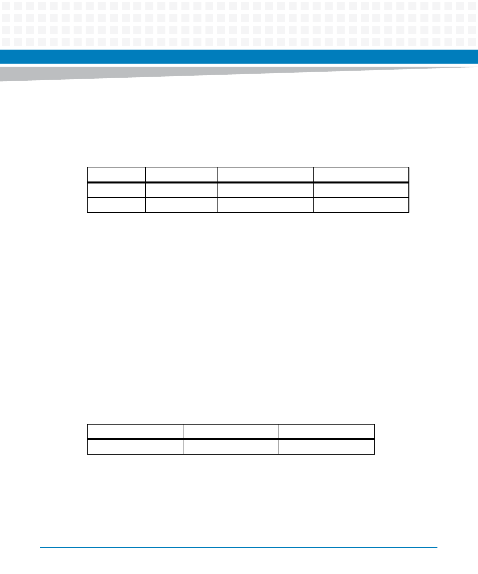
Table 6-6 LPC I/O Register Map Overview
Base Address
Address Size
Address Range Name
Description
0x80
1
POSTCODE
POST Code Register
0x600
128
REGISTERS
FPGA Registers
Table 6-7 IPMC SPI Register
SPI Address Range
Address Range Name
Description
0x00 - 0x7F
REGISTERS
FPGA Registers