4 fpga register mapping, 1 lpc i/o register map, 2 ipmc spi register map – Artesyn ATCA-7470 Installation and Use (October 2014) User Manual
Page 150: 1 lpc i/o register map 6.4.2 ipmc spi register map, Table 6-9, Fpga register map overview, Maps and registers
Maps and Registers
ATCA-7470 Installation and Use (6806800P15K)
150
6.4
FPGA Register Mapping
6.4.1
LPC I/O Register Map
The FPGA registers can be accessed via LPC I/O cycles in the I/O address range REGISTERS. See
Table "FPGA Register Map Overview" on page 150
. For LPC register access, use the base address
0x600 and add the Address Offset. An LPC I/O write access to an address not listed in this table
or not marked with an “X” in the LPC I/O column is ignored. A corresponding read access
delivers always zero.
Note: LPC I/O Address = 0x600 + Address Offset
6.4.2
IPMC SPI Register Map
The FPGA registers may be accessed via IPMC SPI transactions (with the signal
IPMC_SPI_SS_FPGA_ asserted). See
Table "FPGA Register Map Overview" on page 150
. An SPI
write access to an address not listed in this table or not marked with an "X" in the IPMC SPI
column is ignored. A corresponding read access delivers always zero. The address offsets not
mentioned below are not used.
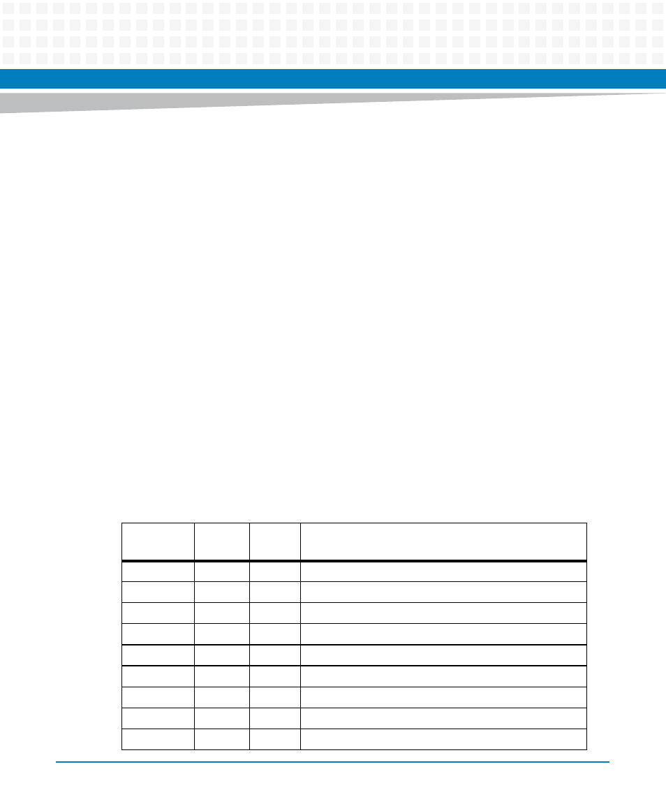
Table 6-9 FPGA Register Map Overview
Address
Offset
1
LPC I/O
IPMC
SPI
Description
0x00
x
x
Module Identification Register
0x01
x
x
FPGA Version Register
0x02
-
-
Reserved / Not used
0x03
x
x
Serial Redirection Control Register
0x04
x
x
SOL Control Register
0x05
x
x
Serial Line Routing Registers
0x06
x
x
Reserved
0x07
Reserved
0x08
x
x
RTM SPI Address/Command Register