Dprx_ber_control, Dprx_ber_control -5 – Altera DisplayPort MegaCore Function User Manual
Page 156

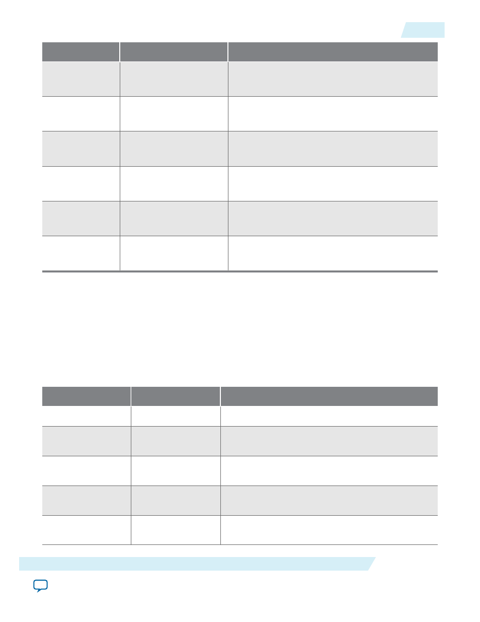
Bit
Bit Name
Function
5
SYM_LOCK1
0 = Symbol unlocked (lane 1)
1 = Symbol locked (lane 1)
4
SYM_LOCK0
0 = Symbol unlocked (lane 0)
1 = Symbol locked (lane 0)
3
CR_LOCK3
0 = Clock unlocked (lane 3)
1 = Clock locked (lane 3)
2
CR_LOCK2
0 = Clock unlocked (lane 2)
1 = Clock locked (lane 2)
1
CR_LOCK1
0 = Clock unlocked (lane 1)
1 = Clock locked (lane 1)
0
CR_LOCK0
0 = Clock unlocked (lane 0)
1 = Clock locked (lane 0)
DPRX_BER_CONTROL
Address: 0×0002
Direction: CRW
Reset: 0×00000000
Note: When
PHY_SINK_TEST_LANE_EN
equals 1,
CR_LOCK
and
SYM_LOCK
bits (register
DPRX_RX_STATUS
)
are forced to 1 for lanes that are not being tested.
Table 10-6: DPRX_BER_CONTROL Bits
Bit
Bit Name
Function
31:28
Unused
27
RSTI3
Writing this bit at 1 resets lane 3 bit-error counter in
register
DPRX_BER_CNTI1
. Always reads as ‘0’.
26
RSTI2
Writing this bit at 1 resets lane 2 bit-error counter in
register
DPRX_BER_CNTI1
. Always reads as ‘0’.
25
RSTI1
Writing this bit at 1 resets lane 1 bit-error counter in
register
DPRX_BER_CNTI0
. Always reads as ‘0’.
24
RSTI0
Writing this bit at 1 resets lane 0 bit-error counter in
register
DPRX_BER_CNTI0
. Always reads as ‘0’.
UG-01131
2015.05.04
DPRX_BER_CONTROL
10-5
DisplayPort Sink Register Map and DPCD Locations
Altera Corporation
