Altera DDR SDRAM High-Performance Controllers and ALTMEMPHY IP User Manual
Page 86
5–40
Chapter 5: Functional Description—ALTMEMPHY
PHY-to-Controller Interfaces
External Memory Interface Handbook Volume 3
June 2011
Altera Corporation
Section I. DDR and DDR2 SDRAM Controllers with ALTMEMPHY IP User Guide
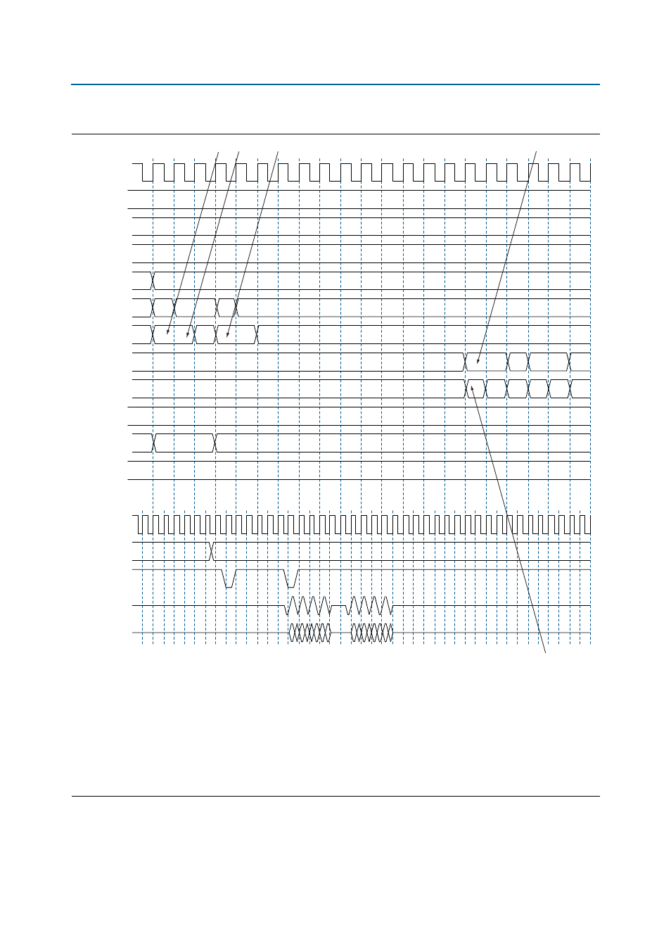
Figure 5–18. Word-Aligned Reads
Notes to
Figure 5–18
:
(1) For AFI, ctl_doing_rd is required to be asserted one memory clock cycle before chip select (ctl_cs_n) is asserted. In the half-rate ctl_clk
domain, this requirement manifests as the controller driving 11 (as opposed to the 01) on ctl_doing_rd.
(2) AFI requires that ctl_doing_rd is driven for the duration of the read. In this example, it is driven to 11 for two half-rate ctl_clks, which equates
to driving to 1, for the four memory clock cycles of this four-beat burst.
(3) The ctl_rdata_valid returns 15 (ctl_rlat) controller clock (ctl_clk) cycles after ctl_doing_rd is asserted. Returned is when the
ctl_rdata_valid
signal is observed at the output of a register within the controller. A controller can use the ctl_rlat value to determine when
to register to returned data, but this is unnecessary as the ctl_rdata_valid is provided for the controller to use as an enable when registering
read data.
(4) Observe the alignment of returned read data with respect to data on the bus.
ctl_clk
ctl_rlat
ctl_ras_n
ctl_cas_n
ctl_we_n
ctl_cs_n
ctl_doing_rd
ctl_rdata_valid
ctl_rdata
ctl_ba
ctl_addr
ctl_dm
Memory
Interface
mem_clk
command
mem_cs_n
mem_dqs
mem_dq
15
11
0
00
00
11
11
11
01
11
01
11
00
00
11
00
11
00
00
00
11
00
11
00
FFFFFFFF
FFFFFFFF
00
0000000
0020008
ACT
RD
(1)
( 2)
(3)
(3)
(4)