Altera DDR SDRAM High-Performance Controllers and ALTMEMPHY IP User Manual
Page 119
Chapter 6: Functional Description—High-Performance Controller II
6–25
Register Maps
June 2011
Altera Corporation
External Memory Interface Handbook Volume 3
Section I. DDR and DDR2 SDRAM Controllers with ALTMEMPHY IP User Guide
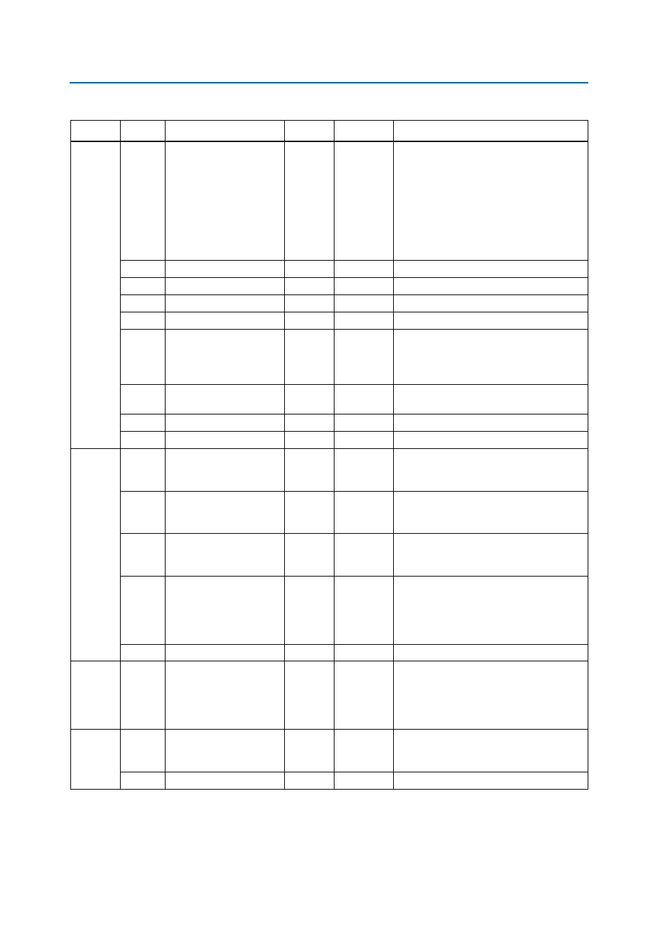
0x110
15:0
AUTO_PD_CYCLES
0x0
Read write
The number of idle clock cycles after which
the controller should place the memory into
power-down mode. The controller is
considered to be idle if there are no
commands in the command queue. Setting
this register to 0 disables the auto
power-down mode. The default value of this
register depends on the values set during the
generation of the design.
16
Reserved.
0
—
Reserved for future use.
17
Reserved.
0
—
Reserved for future use.
18
Reserved.
0
—
Reserved for future use.
19
Reserved.
0
—
Reserved for future use.
21:20
ADDR_ORDER
00
Read write
00 - Chip, row, bank, column.
01 - Chip, bank, row, column.
10 - reserved for future use.
11 - Reserved for future use.
22
REGDIMM
0
Read write
Setting this bit to 1 enables REGDIMM
support in the controller.
24:23
Reserved.
0
—
Reserved for future use.
30:24
Reserved
0
—
Reserved for future use.
0x120
7:0
Column address width
—
Read write
The number of column address bits for the
memory devices in your memory interface.
The range of legal values is 7-12.
15:8
Row address width
—
Read write
The number of row address bits for the
memory devices in your memory interface.
The range of legal values is 12-16.
19:16
Bank address width
—
Read write
The number of bank address bits for the
memory devices in your memory interface.
The range of legal values is 2-3.
23:20
Chip select address width
—
Read write
The number of chip select address bits for
the memory devices in your memory
interface. The range of legal values is 0-2. If
there is only one single chip select in the
memory interface, set this bit to 0.
31:24
Reserved.
0
—
Reserved for future use.
0x121
31:0
Data width representation
(word)
—
Read only
The number of DQS bits in the memory
interface. This bit can be used to derive the
width of the memory interface by multiplying
this value by the number of DQ pins per DQS
pin (typically 8).
0x122
7:0
Chip select representation
—
Read only
The number of chip select in binary
representation. For example, a design with 2
chip selects has the value of 00000011.
31:8
Reserved.
0
—
Reserved for future use.
Table 6–15. Controller Register Map (Part 2 of 5)
Address
Bit
Name
Default
Access
Description