Altera DDR SDRAM High-Performance Controllers and ALTMEMPHY IP User Manual
Page 65
Chapter 5: Functional Description—ALTMEMPHY
5–19
Block Description
June 2011
Altera Corporation
External Memory Interface Handbook Volume 3
Section I. DDR and DDR2 SDRAM Controllers with ALTMEMPHY IP User Guide
You must choose a PLL and PLL input clock pin that are located on the same side of
the device as the memory interface to ensure minimal jitter. Cascaded PLLs are not
recommended as jitter can accumulate, causing the memory output clock to violate
the memory device jitter specification. Also, ensure that the input clock to the PLL is
stable before the PLL locks. If not, you must perform a manual PLL reset (by driving
the global_reset_n signal low) and relock the PLL to ensure that the phase
relationship between all PLL outputs are properly set. The PLL restrictions in half-rate
designs also applies to full-rate designs.
DLL
DLL settings are set depending on the memory clock frequency of operation.
f
For more information on the DLL, refe
chapter in volume 1 of the Stratix III Device Handbook
er in volume 1 of the Stratix IV Device Handbook.
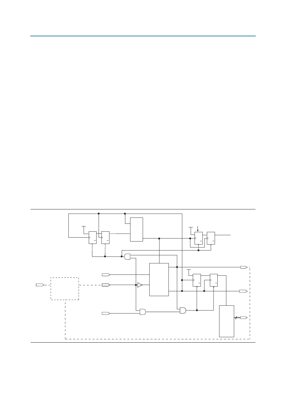
Reset Management
Figure 5–4
shows the main features of the reset management block for the DDR3
SDRAM PHY. You can use the pll_ref_clk input to feed the optional
reset_request_n
edge detect and reset counter module. However, this requires the
pll_ref_clk
signal to use a global clock network resource.
There is a unique reset metastability protection circuit for the clock divider circuit
because the phy_clk domain reset metastability protection registers have fan-in from
the soft_reset_n input so these registers cannot be used.
Figure 5–4. ALTMEMPHY Reset Management Block for Stratix IV and Stratix III Devices
PLL
Q
Q
SET
CLR
D
Q
Q
SET
CLR
D
Q
Q
SET
CLR
D
Q
Q
SET
CLR
D
Q
Q
SET
CLR
D
Q
Q
SET
CLR
D
soft_reset_n
global_reset_n
pll_ref_clk
phy_clk_out
reset_request_n
phy_internal_reset_n
areset
(active HIGH)
pll_reconfig_reset_ams_n
pll_reconfig_reset_ams_n_r
refclk
c0
locked
reset_master_ams
global_pre_clear
Reset
Pipes
PHY resets
pll_reset
pll_locked
Internal reset signal
signal for the
PLL clock-domain
crossing registers
Optional
reset_request_n
edge detect and
reset counter, not
created by the PHY
clk_divider_reset_n
clk
divider
circuit
phy_clk
reset_n
scan_clk
clk_div_reset_ams_n
clk_div_reset_ams_n_r
pll_reconfig_reset_n
global_or_soft_reset_n
Another
system
clock