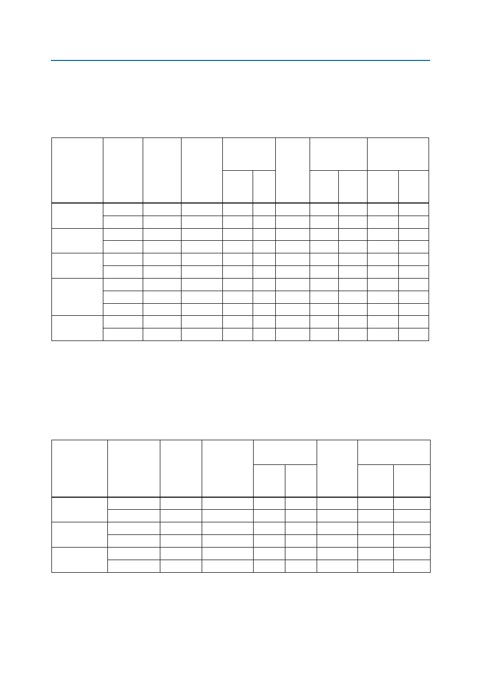
Table 7–3, Table 7–4, Show a typical latency that – Altera DDR SDRAM High-Performance Controllers and ALTMEMPHY IP User Manual
Page 126
7–4
Chapter 7: Latency
External Memory Interface Handbook Volume 3
June 2011
Altera Corporation
Section I. DDR and DDR2 SDRAM Controllers with ALTMEMPHY IP User Guide
The CAS and write latencies are different between DDR and DDR2 SDRAM
interfaces. To calculate latencies for DDR SDRAM interfaces, use the numbers from
DDR2 SDRAM listed below and replace the CAS and write latency with the DDR
SDRAM values.
Table 7–3. Typical Read Latency in HPC II
Device
Frequency
(MHz)
Interface
Controller
Latency
Address and
Command
Latency
CAS
Latency
Read Data
Latency
Total Read
FPGA
I/O
FPGA
I/O
Local
Clock
Cycles
Time
(ns)
Arria GX
233 Half-rate
5
3
1
2
4.5
1
18
154
167
Full-rate
5
2
1
4
5
1
19
114
Arria II GX
233 Half-rate
5
3
1
2.5
5.5
1
18
154
167
Full-rate
5
2
1
4
6
1
20
120
Cyclone III and
Cyclone IV
200 Half-rate
5
3
1
2
4.5
1
18
180
167
Full-rate
5
2
1
4
5
1
19
114
Stratix II and
Stratix II GX
333
Half-rate
5
3
1
2
4.5
1
18
108
267 Half-rate
5
3
1
2
4.5
1
18
135
200 Full-rate
5
2
1
4
5
1
19
95
Stratix III and
Stratix IV
400
Half-rate
5
3
1
2.5
7.125
1.5
20
100
267
Full-rate
4
2
1.5
4
7
1
20
75
Notes to
:
(1) These are typical latency values using the assumptions listed in the beginning of the section. Your actual latency may be different than shown.
Perform your own simulation for your actual latency.
(2) Numbers shown may have been rounded up to the nearest higher integer.
(3) The controller latency value is from the Altera high-performance controller.
(4) CAS latency is per memory device specification and is programmable in the MegaWizard Plug-In Manager.
(5) Total read latency is the sum of controller, address and command, CAS, and read data latencies.
Table 7–4. Typical Write Latency in HPC II
(Part 1 of 2)
Device
Frequency
(MHz)
Interface
Controller
Latency
Address and
Command Latency
Memory
Write
Latency
Total Write
Latency
FPGA
I/O
Local
Clock
Cycles
Time
(ns)
Arria GX
233
Half-rate
5
3
1
1.5
12
103
167
Full-rate
5
2
1
3
12
72
Arria II GX
233
Half-rate
5
3
1
2.5
12
103
167
Full-rate
5
2
1
4
12
72
Cyclone III and
Cyclone IV
200
Half-rate
5
3
1
1.5
12
120
167
Full-rate
5
2
1
3
12
72