Altera DDR SDRAM High-Performance Controllers and ALTMEMPHY IP User Manual
Page 125
Chapter 7: Latency
7–3
June 2011
Altera Corporation
External Memory Interface Handbook Volume 3
Section I. DDR and DDR2 SDRAM Controllers with ALTMEMPHY IP User Guide
Similarly, the write latency in the high-performance controller II is made up of three
components:
write latency = controller latency (T1) + write data latency (T2+T3)
You can separate the controller and ALTMEMPHY read data input latency into
latency that occurred in the I/O element (IOE) and latency that occurred in the FPGA
fabric.
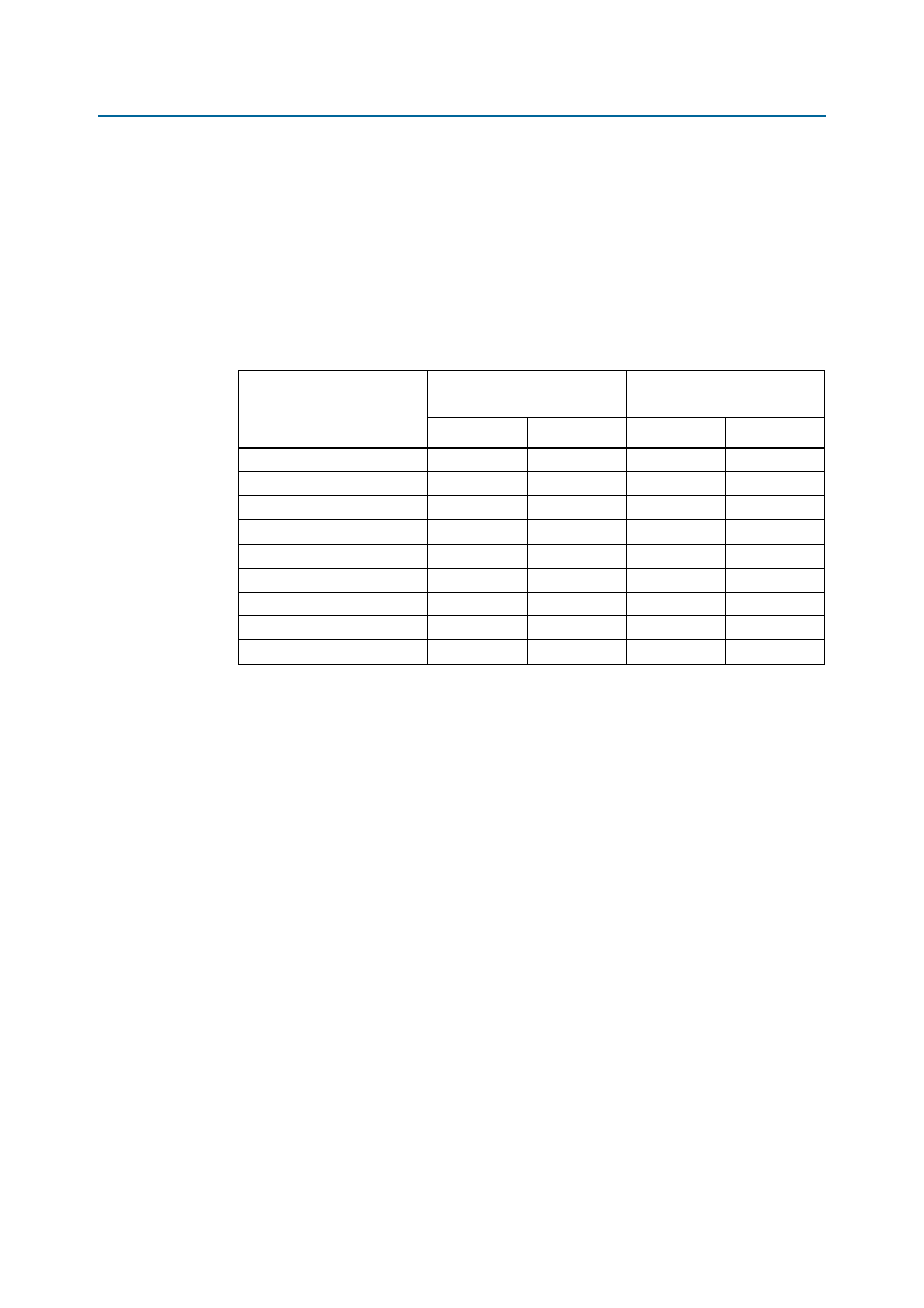
shows the minimum and maximum supported CAS latency for the DDR
and DDR2 SDRAM high-performance controller II.
show a typical latency that can be achieved in Arria GX, Arria
II GX, Cyclone III, Cyclone IV, Stratix IV, Stratix III, Stratix II, and Stratix II GX
devices. The exact latency for your memory controller depends on your precise
configuration. You can obtain precise latency from simulation, but this figure can vary
slightly in hardware because of the automatic calibration process.
The actual memory CAS and write latencies shown are halved in half-rate designs as
the latency calculation is based on the local clock.
The read latency also depends on your board trace delay. The latency found in
simulation can be different from that found in board testing as functional simulation
does not take into account the board trace delays. For a given design on a given board,
the latency may change by one clock cycle (for full-rate designs) or two clock cycles
(for half-rate designs) upon resetting the board. Different boards could also show
different latencies even with the same design.
Table 7–2. Supported CAS Latency
Device Family
Minimum Supported
CAS Latency
Maximum Supported CAS
Latency
DDR
DDR2
DDR
DDR2
Arria GX
3.0
3.0
3.0
6.0
Arria II GX
3.0
3.0
3.0
6.0
Cyclone III
2.0
3.0
3.0
6.0
Cyclone IV
2.0
3.0
3.0
6.0
HardCopy III
3.0
3.0
3.0
6.0
HardCopy IV
3.0
3.0
3.0
6.0
Stratix II
3.0
3.0
3.0
6.0
Stratix III
3.0
3.0
3.0
6.0
Stratix IV
3.0
3.0
3.0
6.0
Note to
(1) The registered DIMMs, where supported, effectively introduce one extra cycle of CAS latency. For the registered
DIMMs, you need to subtract 1.0 from the CAS figures to determine the minimum supported CAS latency, and add
1.0 to the CAS figures to determine the maximum supported CAS latency.