Altera DDR SDRAM High-Performance Controllers and ALTMEMPHY IP User Manual
Page 31
Chapter 3: Parameter Settings
3–5
ALTMEMPHY Parameter Settings
June 2011
Altera Corporation
External Memory Interface Handbook Volume 3
Section I. DDR and DDR2 SDRAM Controllers with ALTMEMPHY IP User Guide
Table 3–3
through
Table 3–5
describe the DDR2 SDRAM parameters available for
memory attributes, initialization options, and timing parameters. DDR SDRAM has
the same parameters, but their value ranges are different than DDR2 SDRAM.
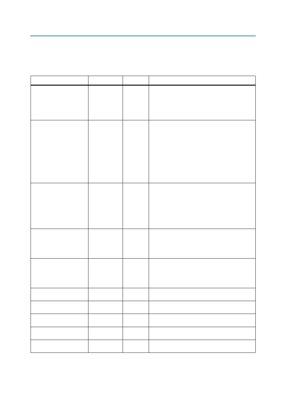
Table 3–3. DDR2 SDRAM Attributes Settings (Part 1 of 2)
Parameter Name
Range
(1)
Units
Description
Output clock pairs from FPGA
1–6
pairs
Defines the number of differential clock pairs driven from
the FPGA to the memory. More clock pairs reduce the
loading of each output when interfacing with multiple
devices. Memory clock pins use the signal splitter feature
in Arria II GX, Stratix III, and Stratix IV devices for
differential signaling.
Total Memory chip selects
1, 2, 4, or 8
bits
Sets the number of chip selects in your memory
interface. The number of chip selects defines the depth of
your memory. You are limited to the range shown as the
local side binary encodes the chip select address. You
can set this value to the next higher number if the range
does not meet your specifications. However, the highest
address space of the ALTMEMPHY megafunction is not
mapped to any of the actual memory address. The
ALTMEMPHY megafunction works with multiple chip
selects and calibrates against all chip select, mem_cs_n
signals.
Memory interface DQ width
? 4–288
bits
Defines the total number of DQ pins on the memory
interface. If you are interfacing with multiple devices,
multiply the number of devices with the number of DQ
pins per device. Even though the GUI allows you to
choose 288-bit DQ width, the interface data width is
limited by the number of pins on the device. For best
performance, have the whole interface on one side of the
device.
Memory vendor
JEDEC, Micron,
Qimonda,
Samsung, Hynix,
Elpida, Nanya,
other
—
Lists the name of the memory vendor for all supported
memory standards.
Memory format
Discrete Device,
Unbuffered
DIMM,
Registered
DIMM
—
Specifies whether you are interfacing with devices or
modules. SODIMM is supported under unbuffered or
registered DIMMs.
Maximum memory frequency
See the memory
device datasheet
MHz
Sets the maximum frequency supported by the memory.
Column address width
9–11
bits
Defines the number of column address bits for your
interface.
Row address width
13–16
bits
Defines the number of row address bits for your
interface.
Bank address width
2 or 3
bits
Defines the number of bank address bits for your
interface.
Chip selects per DIMM
1 or 2
bits
Defines the number of chip selects on each DIMM in your
interface.