Altera DDR SDRAM High-Performance Controllers and ALTMEMPHY IP User Manual
Page 83
Chapter 5: Functional Description—ALTMEMPHY
5–37
PHY-to-Controller Interfaces
June 2011
Altera Corporation
External Memory Interface Handbook Volume 3
Section I. DDR and DDR2 SDRAM Controllers with ALTMEMPHY IP User Guide
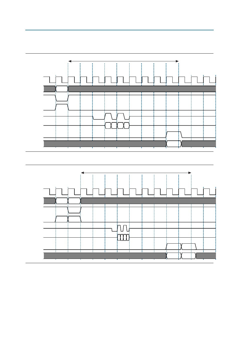
Figure 5–15
shows full-rate reads;
Figure 5–16
shows half-rate reads.
Figure 5–17
and
Figure 5–18
show word-aligned writes and reads. In the following
read and write examples the data is written to and read from the same address. In
each example, ctl_rdata and ctl_wdata are aligned with controller clock (ctl_clk)
cycles. All the data in the bit vector is valid at once. For comparison, refer
Figure 5–19
and
Figure 5–20
that show the word-unaligned writes and reads.
Figure 5–15. Full-Rate Reads
Figure 5–16. Half-Rate Reads
ctl_rlat = 9
1
2
3
4
5
6
7
8
9
clock
ctl_addr
ctl_cs_n
ctl_doing_rd
mem_dqs
mem_dq
ctl_rdata_valid
ctl_rdata
clock
ctl_addr
ctl_cs_n
ctl_doing_rd
mem_dqs
mem_dq
ctl_rdata_valid
ctl_rdata
AX
XA
10
10
01
10
01
DX
XD
ctl_rlat = 9
1
2
3
4
5
6
7
8
9