Altera DDR SDRAM High-Performance Controllers and ALTMEMPHY IP User Manual
Page 60
5–14
Chapter 5: Functional Description—ALTMEMPHY
Block Description
External Memory Interface Handbook Volume 3
June 2011
Altera Corporation
Section I. DDR and DDR2 SDRAM Controllers with ALTMEMPHY IP User Guide
The minimum PHY requirement is to have 48 phases of the highest frequency clock.
The PLL uses Normal mode, unlike other device families. Cyclone III PLL in normal
mode emits low jitter already such that you do not require to set the PLL in the With
No Compensation
option. Changing the PLL compensation mode may result in
inaccurate timing results.
You must choose a PLL and PLL input clock pin that are located on the same side of
the memory interface to ensure minimal jitter. Cascaded PLLs are not recommended
as jitter can accumulate with the use of cascaded PLLs causing the memory output
clock to violate the memory device jitter specification. Also, ensure that the input
clock to the PLL is stable before the PLL locks. If not, you must perform a manual PLL
reset and relock the PLL to ensure that the phase relationship between all PLL outputs
are properly set.
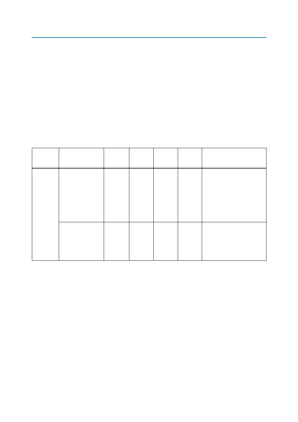
Table 5–3
lists the clocks generated by the ALTPLL megafunction.
Table 5–3. DDR/DDR2 SDRAM Clocking in Cyclone III Devices (Part 1 of 2) (Part 1 of 2)
Design
Rate
Clock Name
Post-Scale
Counter
Phase
(Degrees)
Clock
Rate
Clock
Network
Type
Notes
Half-rate
phy_clk_1x
and
aux_half_rate_cl
k
C0
0
Half-Rate
Global
The only half-rate clock
parameterizable for the
ALTMEMPHY megafunction to
be used by the controller. This
clock is not used in full-rate
controllers. This clock also
feeds into a divider circuit to
provide the PLL scan_clk
signal for reconfiguration.
mem_clk_2x
and
aux_full_
rate_clk
C1
0
Full-Rate
Global
Generates DQS signals and the
memory clock and to clock the
PHY in full-rate mode.