Altera DDR SDRAM High-Performance Controllers and ALTMEMPHY IP User Manual
Page 127
Chapter 7: Latency
7–5
June 2011
Altera Corporation
External Memory Interface Handbook Volume 3
Section I. DDR and DDR2 SDRAM Controllers with ALTMEMPHY IP User Guide
f
To see the latency incurred in the IOE for both read and write paths for ALTMEMPHY
variations in Stratix IV and Stratix III devices refer to the IOE figure
Stratix III Device Handbook and the
chapter of the Stratix IV Device
Handbook.
Stratix II and
Stratix II GX
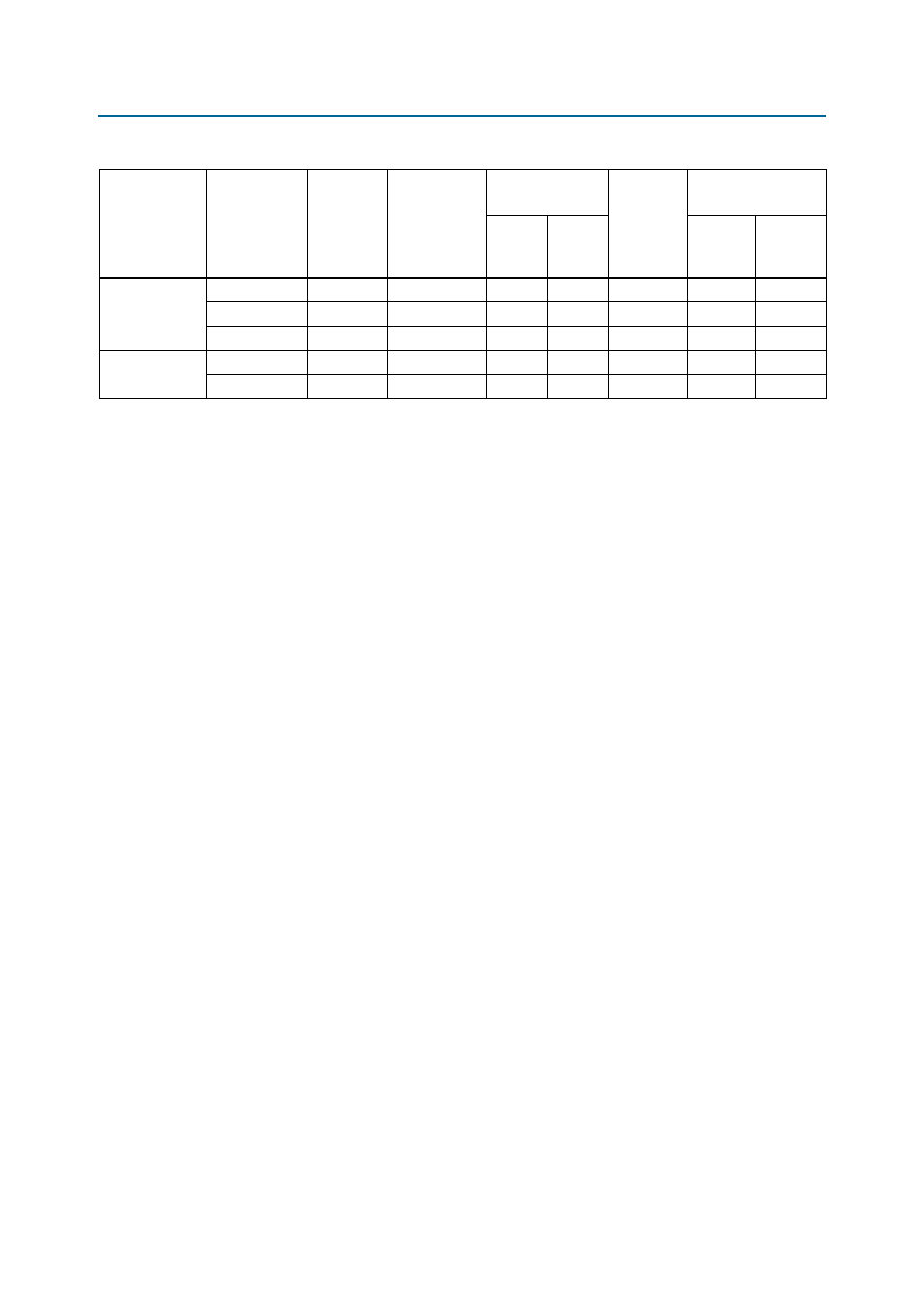
333
Half-rate
5
3
1
1.5
12
72
267
Half-rate
5
3
1
1.5
12
90
200
Full-rate
5
2
1
3
12
60
Stratix III and
Stratix IV
400
Half-rate
5
3
1
2
12
60
267
Full-rate
5
2
1.5
3
13
49
Notes to
:
(1) These are typical latency values using the assumptions listed in the beginning of the section. Your actual latency may be different than shown.
Perform your own simulation for your actual latency.
(2) Numbers shown may have been rounded up to the nearest higher integer.
(3) The controller latency value is from the Altera high-performance controller.
(4) Memory write latency is per memory device specification. The latency from when you provide the command to write to when you need to
provide data at the memory device.
(5) Total write latency is the sum of controller, address and command, and memory write latencies.
Table 7–4. Typical Write Latency in HPC II
(1)
,
(2)
(Part 2 of 2)
Device
Frequency
(MHz)
Interface
Controller
Latency
(3)
Address and
Command Latency
Memory
Write
Latency
(4)
Total Write
Latency
(5)
FPGA
I/O
Local
Clock
Cycles
Time
(ns)