Top-level signals description, Top-level signals description –11 – Altera DDR SDRAM High-Performance Controllers and ALTMEMPHY IP User Manual
Page 105
Chapter 6: Functional Description—High-Performance Controller II
6–11
Top-Level Signals Description
June 2011
Altera Corporation
External Memory Interface Handbook Volume 3
Section I. DDR and DDR2 SDRAM Controllers with ALTMEMPHY IP User Guide
Top-Level Signals Description
Table 6–6
shows the clock and reset signals.
1
The suffix _n denotes active low signals.
Write Data Channel
Avalon-ST Data Slave Interface
Avalon-ST
(2)
Write Data Channel, SCMD.
Read Data Channel
Avalon-ST Data Slave Interface
Avalon-ST
(2)
Read data channel, SCMD with read data
error response.
Controller-PHY Interface
AFI 2.0
AFI Interface
AFI
(1)
Interface between controller and PHY.
Memory Side-Band Signals
Self Refresh (Low Power)
Interface
Self Refresh (Low Power)
Interface
Avalon Control
& Status
Interface
(2)
SDRAM-specific signals to place
memory into low-power mode.
User-Controller Refresh
Interface
User-Controller Refresh
Interface
Avalon Control
& Status
Interface
(2)
SDRAM-specific signals to request
memory refresh.
Configuration and Status Register (CSR) Interface
CSR
Configuration and Status
Register Interface
Avalon-MM
(2)
Enables on-the-fly configuration of
memory timing parameters, address
widths, and controller behaviour.
Notes:
(1) For information about AFI signals, refer to
.
(2) For information about Avalon signals, refer to
.
Table 6–5. Summary of Controller External Interfaces (Part 2 of 2)
Interface Name
Display Name
Type
Description
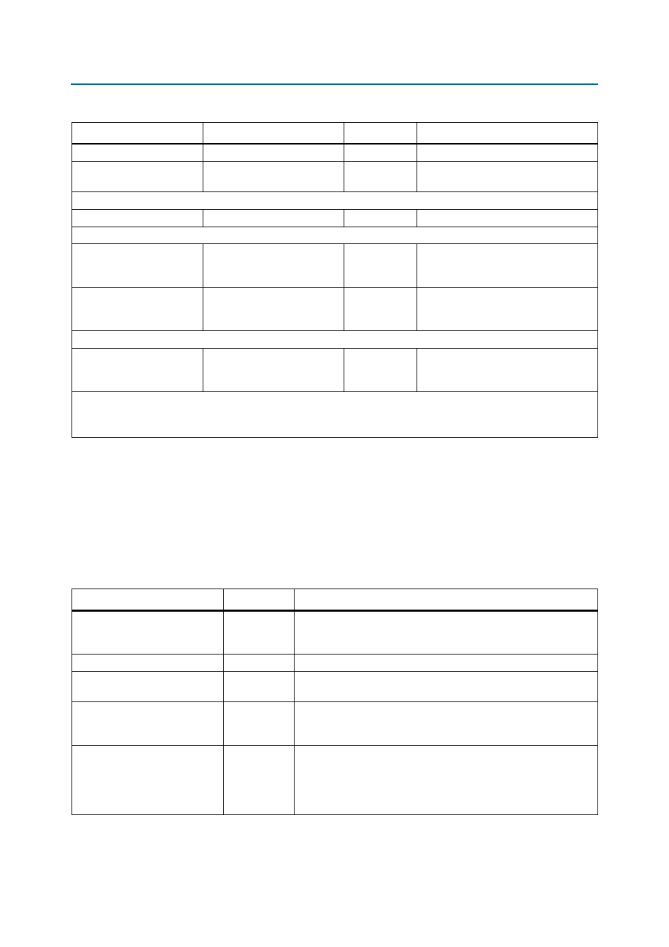
Table 6–6. Clock and Reset Signals (Part 1 of 2)
Name
Direction
Description
global_reset_n
Input
The asynchronous reset input to the controller. The IP core derives all
other reset signals from resynchronized versions of this signal. This
signal holds the PHY, including the PLL, in reset while low.
pll_ref_clk
Input
The reference clock input to PLL.
phy_clk
Output
The system clock that the PHY provides to the user. All user inputs to
and outputs from the controller must be synchronous to this clock.
reset_phy_clk_n
Output
The reset signal that the PHY provides to the user. The IP core asserts
reset_phy_clk_n
asynchronously and deasserts synchronously to
phy_clk
clock domain.
aux_full_rate_clk
Output
An alternative clock that the PHY provides to the user. This clock
always runs at the same frequency as the external memory interface.
In half-rate designs, this clock is twice the frequency of the phy_clk
and you can use it whenever you require a 2x clock. In full-rate
designs, the same PLL output as the phy_clk signal drives this clock.