Rainbow Electronics DS3134 User Manual
Page 62
DS3134
62 of 203
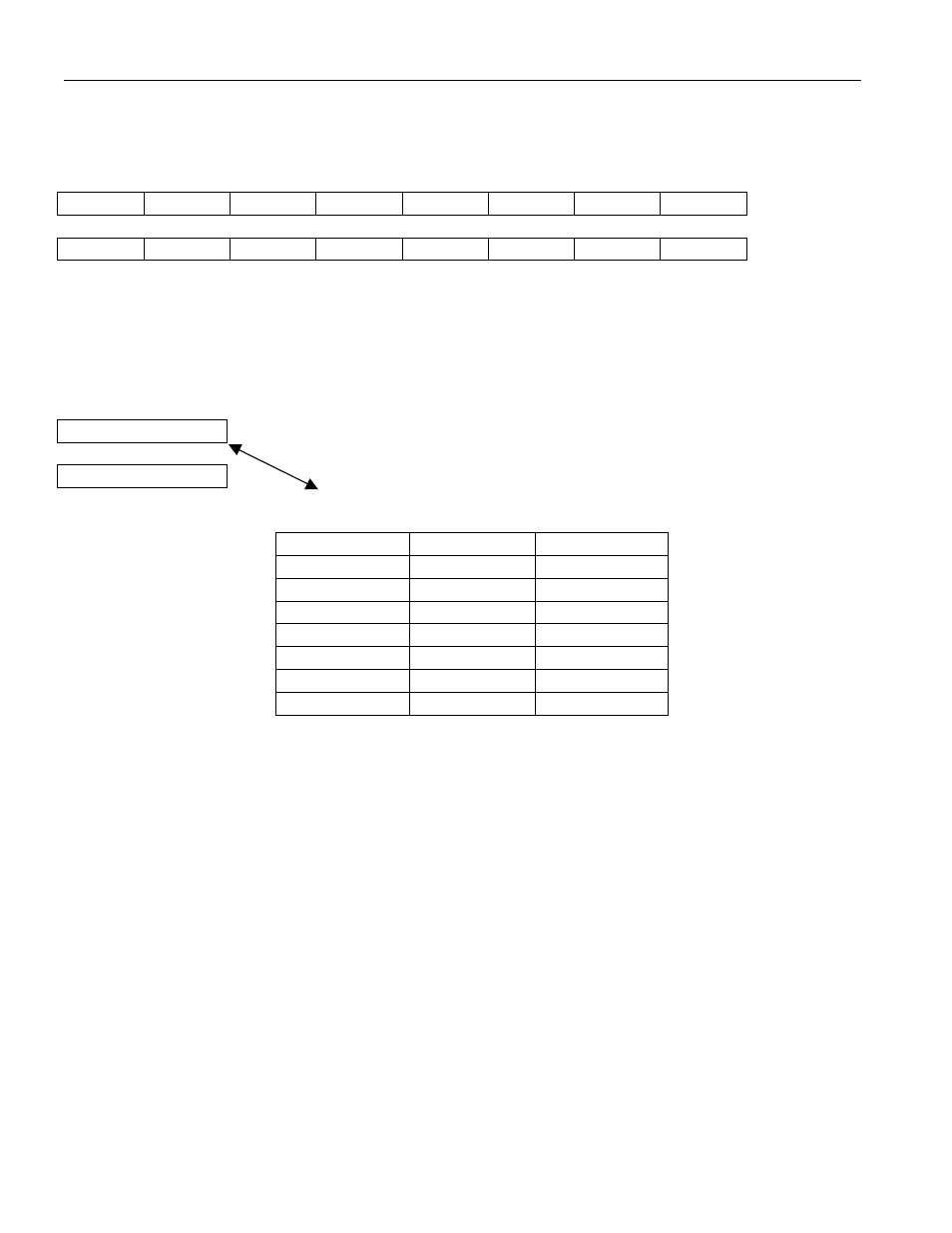
Register Name:
CP[n]RD where n = 0 to 15 for each Port
Register Description: Channelized Port [n] Register Data
Register Address:
See the Register Map in Section 3
7
6
5
4
3
2
1
0
CHD7
CHD6
CHD5
CHD4
CHD3
CHD2
CHD1
CHD0
15
14
13
12
11
10
9
8
CHD15
CHD14
CHD13
CHD12
CHD11
CHD10
CHD9
CHD8
Note: Bits that are underlined are read only, all other bits are read-write; default value for all bits is 0.
Bits 0 to 15 / DS0 Channel Data (CHD0 to CHD15). The 16-bit data that is to either be written into or
read from the PORT RAM specified by the CP[n]RDIS register.
Port RAM Indirect Access Figure 5.3B
CP[n]RDIS
CP[n]RD
Port RAM (one each for all 16 Ports; n = 0 to 15)
C[n]DAT0
R[n]CFG0
T[n]CFG0
C[n]DAT1
R[n]CFG1
T[n]CFG1
C[n]DAT2
R[n]CFG2
T[n]CFG2
C[n]DAT3
R[n]CFG3
T[n]CFG3
C[n]DAT4
R[n]CFG4
T[n]CFG4
...
...
...
C[n]DAT126
R[n]CFG126
T[n]CFG126
C[n]DAT127
R[n]CFG127
T[n]CFG127
- MAX12005 (14 pages)
- MAX7058 (14 pages)
- MAX9995 (13 pages)
- MAX7034 (13 pages)
- MAX7033 (16 pages)
- MAX9476 (8 pages)
- MAX9486 (8 pages)
- MAX14821 (29 pages)
- MAX9489 (11 pages)
- MAX9491 (11 pages)
- DS2130Q (22 pages)
- DS21458 (270 pages)
- DS3131 (174 pages)
- DS26502 (125 pages)
- DS2153Q (48 pages)
- DS26503 (123 pages)
- DS2186 (11 pages)
- DS1842A (6 pages)
- DS1876 (69 pages)
- DS1874 (88 pages)
- DS31256 (181 pages)
- DS2141A (35 pages)
- DS3184 (13 pages)
- DS2154 (69 pages)
- DS26504 (128 pages)
- DS3164 (12 pages)
- DS1852 (25 pages)
- DS2181A (32 pages)
- DS2151Q (46 pages)
- DS1843 (8 pages)
- DS2165Q (17 pages)
- DS3170 (233 pages)
- DS2180A (36 pages)
- DS2172 (20 pages)
- DS2152 (79 pages)
- DS1841 (16 pages)
- DS2182A (22 pages)
- DS2143Q (40 pages)
- DS2132A_Q (17 pages)
- DS1862 (42 pages)
- DS26519 (310 pages)
- DS2188 (11 pages)
- DS1875 (92 pages)
- DS33M33 (20 pages)