Pci write cycle, Pci bus write figure 9.1c – Rainbow Electronics DS3134 User Manual
Page 147
DS3134
147 of 203
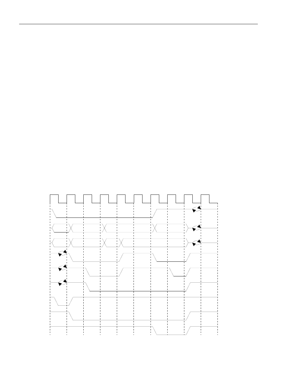
PCI Write Cycle
A write cycle on the PCI bus is shown in Figure 9.1C. During clock cycle #1, the initiator asserts the
PFRAME* signal and drives the address onto the PAD signal lines and the bus command (which would
be a write) onto the PCBE* signal lines. The target reads the address and bus command and if the address
matches it's own, then it will assert the PDEVSEL* signal and begin the bus transaction. During clock
cycle #2, the initiator stops driving the address onto the PAD signal lines and begins driving data #1. It
also switches the PCBE* signal lines to now indicate the byte enable for data #1. The initiator asserts the
PIRDY* signal and begins monitoring the PDEVSEL* and PTRDY* signals. During clock cycle #3, the
initiator detects that PDEVSEL* and PTRDY* are asserted which indicates that the target has accepted
data #1 and the initiator begins driving the data and byte enable for data #2. During clock cycle #4, since
PDEVSEL* and PTRDY* are asserted, data #2 is written by the initiator to the target. During clock cycle
#5, both PIRDY* and PTRDY* are deasserted indicating that neither the initiator nor the target are ready
for data #3 to be passed. During clock cycle #6, the initiator is now ready so it asserts PIRDY* and
deasserts PFRAME* which indicates that data #3 will be the last one passed. During clock cycle #8, the
target asserts PTRDY* which indicates to the initiator that data #3 is ready to be accepted by the target.
During clock cycle #9, the initiator deasserts PIRDY* and stops driving the PAD and PCBE* signal lines.
The target deasserts PDEVSEL* and PTRDY*.
The PXAS*, PXDS*, and PXBLAST* signals are not part of a standard PCI bus. These PCI extension
signals that are unique to the device. They are useful in adapting the PCI bus to a proprietary bus scheme.
They are only asserted when the device is a bus master.
PCI Bus Write Figure 9.1C
1
2
3
4
5
6
7
8
9
10
data #1
Address
CMD
BE #1
PCLK
PFRAME*
PAD
PCBE*
PIRDY*
PTRDY*
PDEVSEL*
PXDS*
PXAS*
PXBLAST*
pci_writ
data #2
data #3
BE #2
BE #3