Rainbow Electronics DS3134 User Manual
Page 56
DS3134
56 of 203
5.2 PORT REGISTER DESCRIPTIONS
Receive Side Control Bits (one each for all 16 ports)
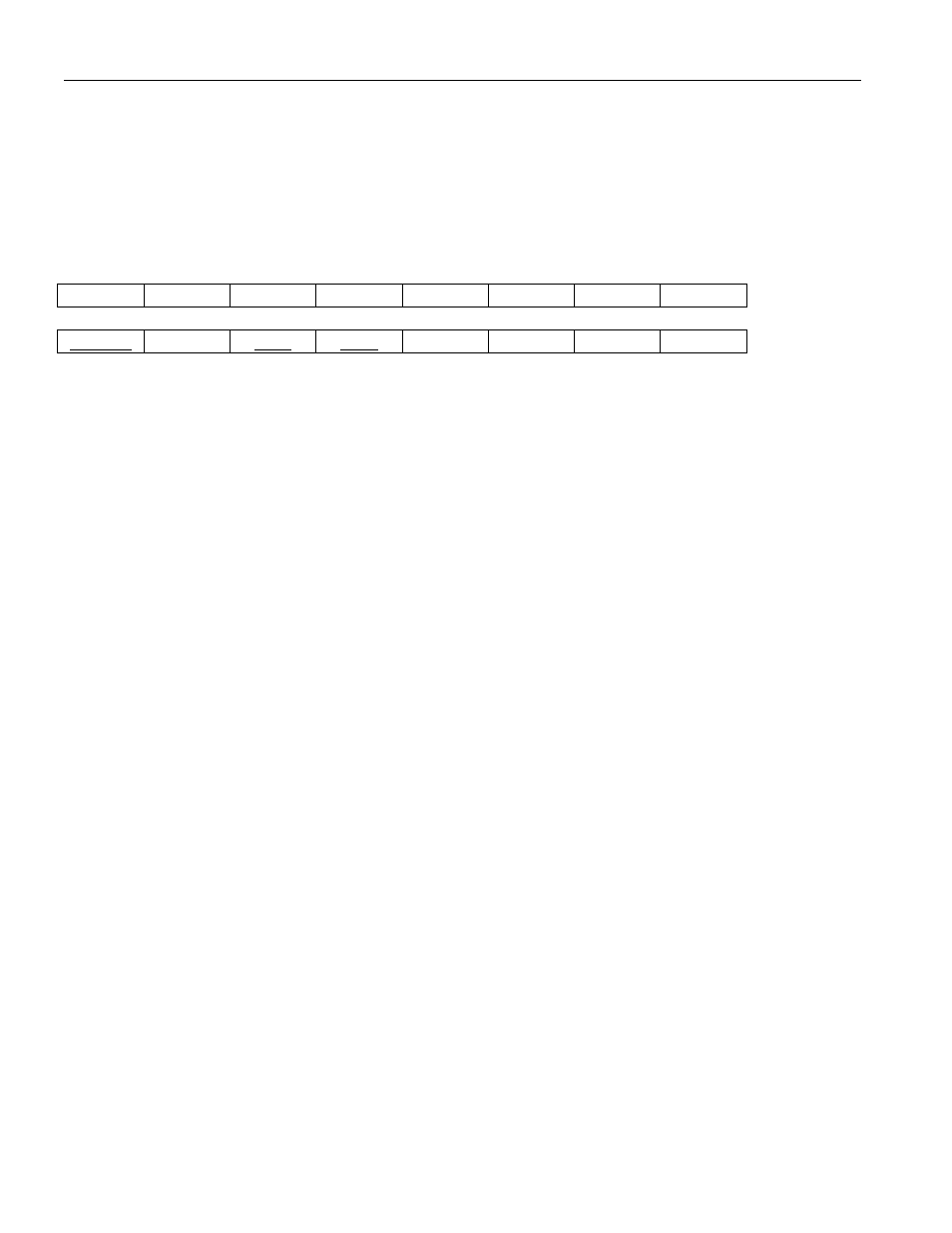
Register Name:
RP[n]CR where n = 0 to 15 for each Port
Register Description: Receive Port [n] Control Register
Register Address:
See the Register Map in Section 3
7
6
5
4
3
2
1
0
RSS1
RSS0
RSD1
RSD0
VRST
RISE
RIDE
RICE
15
14
13
12
11
10
9
8
RCOFA
IERC
VLB
VTO
n/a
LLB
RUEN
RP[i]HS
Note: Bits that are underlined are read only, all other bits are read-write; default value for all bits is 0.
Bit 0 / Invert Clock Enable (RICE).
0 = do not invert clock (normal mode)
1 = invert clock (inverted clock mode)
Bit 1 / Invert Data Enable (RIDE).
0 = do not invert data (normal mode)
1 = invert data (inverted data mode)
Bit 2 / Invert Sync Enable (RISE).
0 = do not invert sync pulse (normal mode)
1 = invert sync pulse (inverted sync pulse mode)
Bit 3 / V.54 Detector Reset (VRST). Toggling this bit from a 0 to a 1 and then back to a 0 causes the
internal V.54 detector to be reset and begin searching for the V.54 loop up pattern. See Section 5.4 for
more details on the operation of the V.54 detector.
Bit 4 / Sync Delay Bit 0 (RSD0).
Bit 5 / Sync Delay Bit 1 (RSD1).
These two bits define the format of the sync signal that will be applied to the RS[n] input. These bits are
ignored if the port has been configured to operate in an unchannelized fashion (RUEN = 1).
00 = sync pulse is 0 clocks early
01 = sync pulse is 1/2 clock early
10 = sync pulse is 1 clock early
11 = sync pulse is 2 clocks early