Rainbow Electronics DS3134 User Manual
Page 16
DS3134
16 of 203
SECTION 2: SIGNAL DESCRIPTION
2.1 OVERVIEW / SIGNAL LEAD LIST
This section describes the input and output signals on the DS3134. Signal names follow a convention that
is shown in Table 2.1A. Table 2.1B lists all of the signals, their signal type, description, and lead
location.
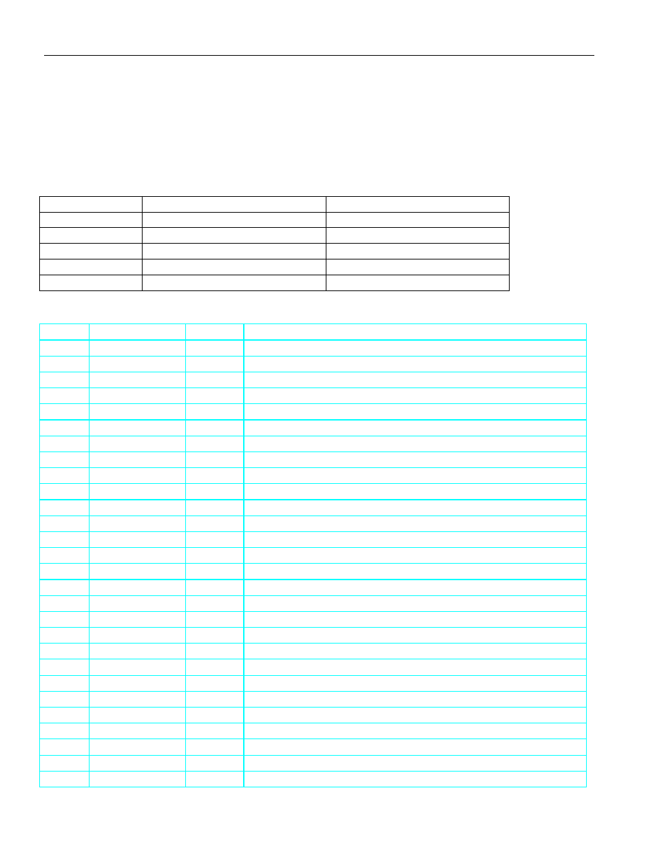
Signal Naming Convention Table 2.1A
First Letter
Signal Category
Section
R
Receive Serial Port
2.2
T
Transmit Serial Port
2.2
L
Local Bus
2.3
J
JTAG Test Port
2.4
P
PCI Bus
2.5
Signal Description / Lead List (sorted by symbol) Table 2.1B
Lead
Symbol
Type
Signal Description
V19
JTCLK
I
JTAG IEEE 1149.1 Test Serial Clock.
U18
JTDI
I
JTAG IEEE 1149.1 Test Serial Data Input.
T17
JTDO
O
JTAG IEEE 1149.1 Test Serial Data Output.
W20
JTMS
I
JTAG IEEE 1149.1 Test Mode Select.
U19
JTRST*
I
JTAG IEEE 1149.1 Test Reset.
G20
LA0
I/O
Local Bus Address Bit 0. LSB.
G19
LA1
I/O
Local Bus Address Bit 1.
F20
LA2
I/O
Local Bus Address Bit 2.
G18
LA3
I/O
Local Bus Address Bit 3.
F19
LA4
I/O
Local Bus Address Bit 4.
E20
LA5
I/O
Local Bus Address Bit 5.
G17
LA6
I/O
Local Bus Address Bit 6.
F18
LA7
I/O
Local Bus Address Bit 7.
E19
LA8
I/O
Local Bus Address Bit 8.
D20
LA9
I/O
Local Bus Address Bit 9.
E18
LA10
I/O
Local Bus Address Bit 10.
D19
LA11
I/O
Local Bus Address Bit 11.
C20
LA12
I/O
Local Bus Address Bit 12.
E17
LA13
I/O
Local Bus Address Bit 13.
D18
LA14
I/O
Local Bus Address Bit 14.
C19
LA15
I/O
Local Bus Address Bit 15.
B20
LA16
I/O
Local Bus Address Bit 16.
C18
LA17
I/O
Local Bus Address Bit 17.
B19
LA18
I/O
Local Bus Address Bit 18.
A20
LA19
I/O
Local Bus Address Bit 19. MSB.
L20
LBGACK*
O
Local Bus Grant Acknowledge.
H20
LBHE*
O
Local Bus Byte High Enable.
J20
LCLK
O
Local Bus Clock.