Pci bus interface ac timing diagram figure 12d – Rainbow Electronics DS3134 User Manual
Page 196
DS3134
196 of 203
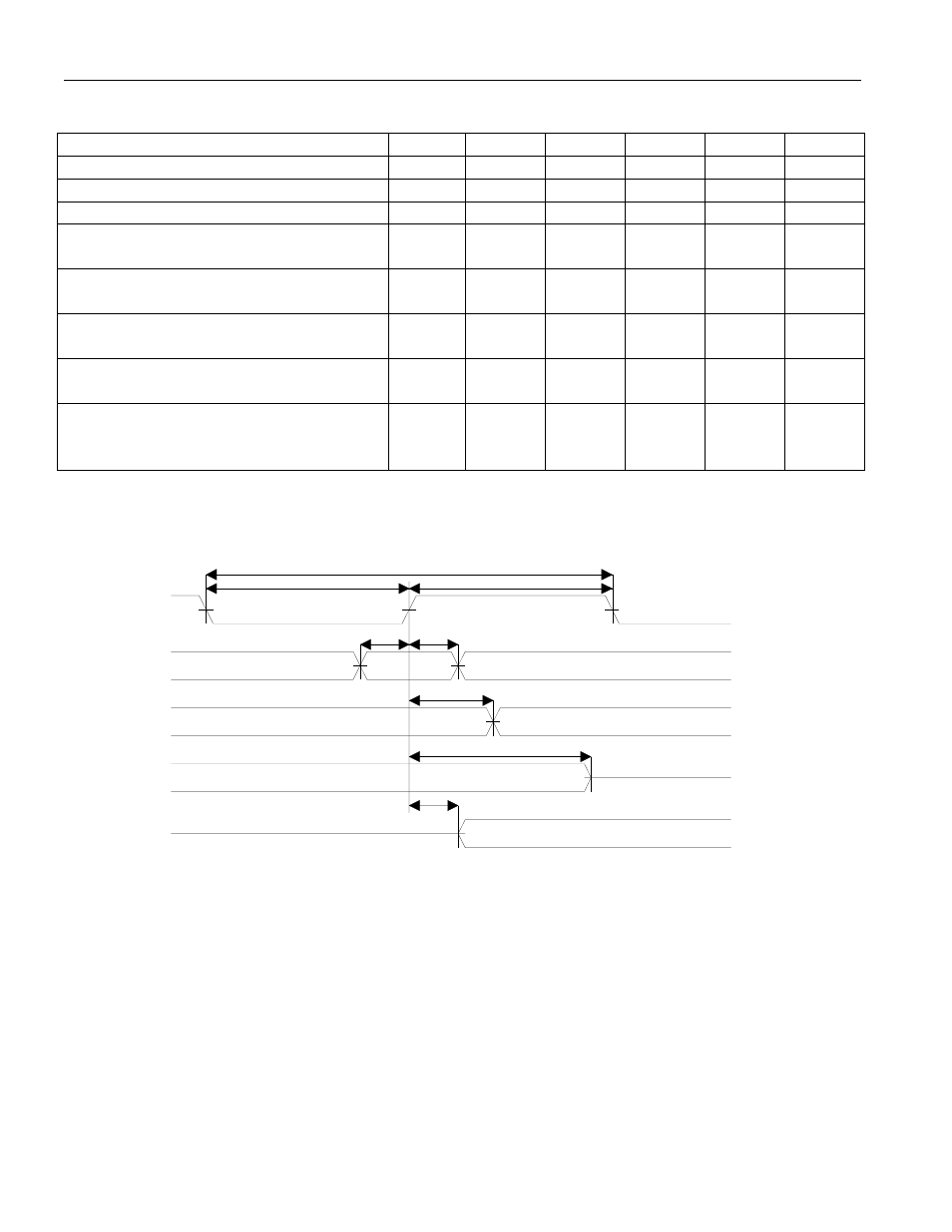
AC CHARACTERISTICS - PCI BUS INTERFACE
(0
°
C TO +70
°
C; VDD = 3.0V TO 3.6V)
Parameter
Symbol
Min
Typ
Max
Units
Notes
PCLK Period
t1
30
40
ns
PCLK Low Time
t2
12
ns
PCLK High Time
t3
12
ns
All PCI Inputs & I/O Set Up Time to the
Rising Edge of PCLK
t4
7
ns
All PCI Inputs & I/O Hold Time from the
Rising Edge of PCLK
t5
0
ns
Delay from the Rising Edge of PCLK to
Data Valid on all PCI Outputs & I/O
t6
2
11
ns
Delay from the Rising Edge of PCLK to
Tri-State on all PCI Outputs & I/O
t7
28
ns
Delay from the Rising Edge of PCLK to
Data Valid from Tri-State on all PCI
Outputs & I/O
t8
2
ns
PCI BUS INTERFACE AC TIMING DIAGRAM Figure 12D
Data Valid
PCLK
PCI Input
& I/O
PCI Output
& I/O
PCI Output &
I/O to Tri-State
PCI Output &
I/O from Tri-State
Data Valid
Tri-State
Tri-State
t4
t5
t6
t7
t8
t1
t2
t3
pci_ac
- MAX12005 (14 pages)
- MAX7058 (14 pages)
- MAX9995 (13 pages)
- MAX7034 (13 pages)
- MAX7033 (16 pages)
- MAX9476 (8 pages)
- MAX9486 (8 pages)
- MAX14821 (29 pages)
- MAX9489 (11 pages)
- MAX9491 (11 pages)
- DS2130Q (22 pages)
- DS21458 (270 pages)
- DS3131 (174 pages)
- DS26502 (125 pages)
- DS2153Q (48 pages)
- DS26503 (123 pages)
- DS2186 (11 pages)
- DS1842A (6 pages)
- DS1876 (69 pages)
- DS1874 (88 pages)
- DS31256 (181 pages)
- DS2141A (35 pages)
- DS3184 (13 pages)
- DS2154 (69 pages)
- DS26504 (128 pages)
- DS3164 (12 pages)
- DS1852 (25 pages)
- DS2181A (32 pages)
- DS2151Q (46 pages)
- DS1843 (8 pages)
- DS2165Q (17 pages)
- DS3170 (233 pages)
- DS2180A (36 pages)
- DS2172 (20 pages)
- DS2152 (79 pages)
- DS1841 (16 pages)
- DS2182A (22 pages)
- DS2143Q (40 pages)
- DS2132A_Q (17 pages)
- DS1862 (42 pages)
- DS26519 (310 pages)
- DS2188 (11 pages)
- DS1875 (92 pages)
- DS33M33 (20 pages)