Rainbow Electronics DS3134 User Manual
Page 51
DS3134
51 of 203
Bit 11 / Status Bit for Receive DMA Done Queue Write Error (RDQWE).
0 = interrupt masked
1 = interrupt unmasked
Bit 12 / Status Bit for Transmit FIFO Underflow (TUDFL).
0 = interrupt masked
1 = interrupt unmasked
Bit 13 / Status Bit for Transmit DMA Pending Queue Read (TPQR).
0 = interrupt masked
1 = interrupt unmasked
Bit 14 / Status Bit for Transmit DMA Done Queue Write (TDQW).
0 = interrupt masked
1 = interrupt unmasked
Bit 15 / Status Bit for Transmit DMA Done Queue Write Error (TDQWE).
0 = interrupt masked
1 = interrupt unmasked
4.4 TEST REGISTER DESCRIPTION
Register Name:
TEST
Register Description: Test Register
Register Address:
0050h
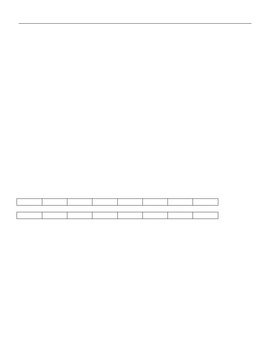
7
6
5
4
3
2
1
0
n/a
n/a
n/a
n/a
n/a
n/a
n/a
FT
15
14
13
12
11
10
9
8
n/a
n/a
n/a
n/a
n/a
n/a
n/a
n/a
Note: Bits that are underlined are read only, all other bits are read-write; default value for all bits is 0.
Bit 0 / Factory Test (FT).
This bit is used by the factory to place the DS3134 into the test mode. For normal device operation, this
bit should be set to zero whenever this register is written to. Setting this bit places the RAMs into a low
power standby mode.
Bit 1 to 15 / Device internal test bits. Bits 1 to 15 shown in the above table is for CHATEAU internal
(Dallas Semiconductor) tests use, not user test mode controls. Values of these bits should always be “0”.
If any of these bits are set to “1” device will not function properly.