Rainbow Electronics DS3134 User Manual
Page 115
DS3134
115 of 203
Done Queue FIFO Flush Timer
To make sure that the Done Queue FIFO does get flushed to the Done Queue on a regular basis, the
Receive Done Queue FIFO Flush Timer (RDQFFT) is used by the DMA to determine the maximum wait
time in between writes. The RDQFFT is a 16-bit programmable counter that is decremented every PCLK
divided by 256. It is only monitored by the DMA when the Receive Done Queue FIFO is enabled
(RDQFE = 1). For a 33 MHz PCLK, the timer is decremented every 7.76 us and for a 25 MHz clock it is
decremented every 10.24 us. Each time the DMA writes to the Done Queue it resets the timer to the
count placed into it by the Host. On initialization, the Host will set a value into the RDQFFT that
indicates the maximum time the DMA should wait in between writes to the Done Queue. For example,
with a PCLK of 33 MHz, the range of wait times are from 7.8 us (RDQFFT = 0001h) to 508 ms
(RDQFFT = FFFFh) and PCLK of 25 MHz, the wait times range from 10.2 us (RDQFFT = 0001h) to 671
ms (RDQFFT = FFFFh).
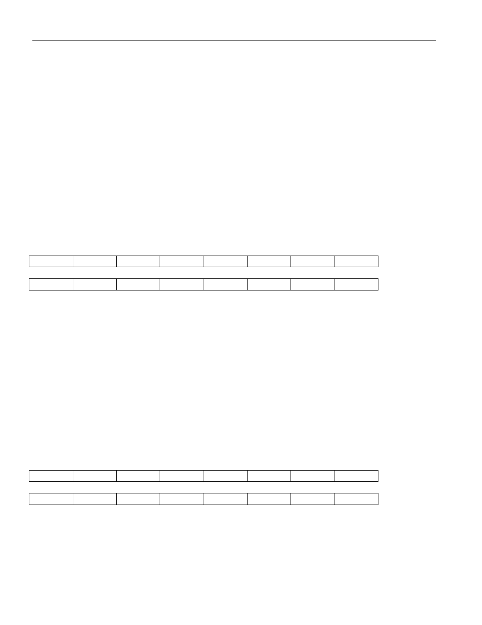
Register Name:
RDQFFT
Register Description: Receive Done Queue FIFO Flush Timer
Register Address:
0744h
7
6
5
4
3
2
1
0
TC7
TC6
TC5
TC4
TC3
TC2
TC1
TC0
15
14
13
12
11
10
9
8
TC15
TC14
TC13
TC12
TC11
TC10
TC9
TC8
Note: Bits that are underlined are read only, all other bits are read-write; default value for all bits is 0.
Bits 0 to 15 / Receive Done Queue FIFO Flush Timer Control Bits (TC0 to TC15). Please note that
on system reset, the timer will be set to 0000h which is defined as an illegal setting. If the Receive Done
Queue FIFO is to be activated (RDQFE = 1), then the Host must first configure the timer to a proper state
and then set the RDQFE bit to one.
0000h = illegal setting
0001h = Timer Count Resets to 1
FFFFh = Timer Count Resets to 65536
Register Name:
RDMAQ
Register Description: Receive DMA Queues Control
Register Address:
0780h
7
6
5
4
3
2
1
0
n/a
n/a
RDQF
RDQFE
RFQSF
RFQLF
n/a
RFQFE
15
14
13
12
11
10
9
8
n/a
n/a
n/a
n/a
n/a
RDQT2
RDQT1
RDQT0
Note: Bits that are underlined are read only, all other bits are read-write; default value for all bits is 0.
Bit 0 / Receive Free Queue FIFO Enable (RFQFE). See Section 8.1.3 for details.
Bit 2 / Receive Free Queue Large Buffer FIFO Flush (RFQLF). See Section 8.1.3 for details.
Bit 3 / Receive Free Queue Small Buffer FIFO Flush (RFQSF). See Section 8.1.3 for details.