Layer one port ac timing diagram figure 12a – Rainbow Electronics DS3134 User Manual
Page 191
DS3134
191 of 203
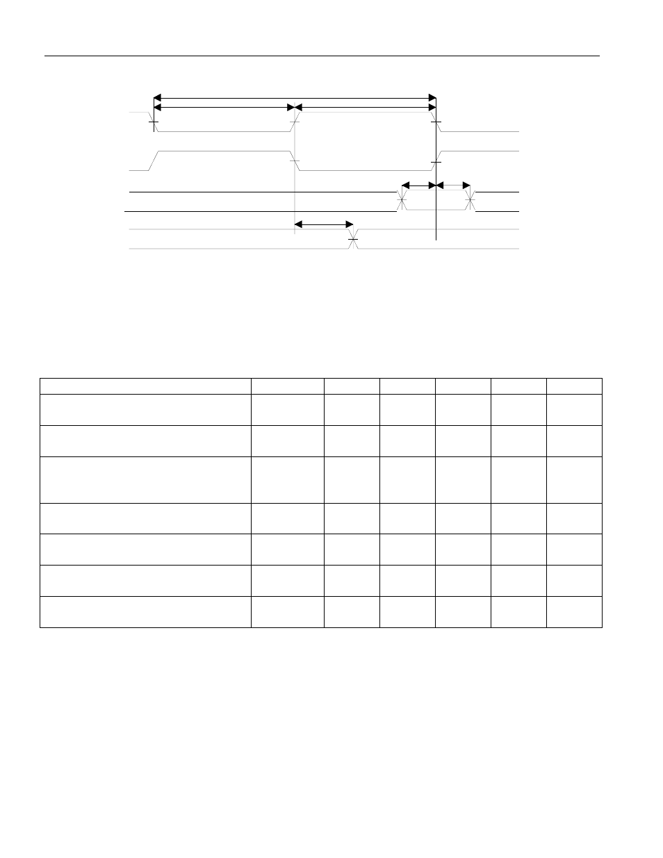
LAYER ONE PORT AC TIMING DIAGRAM Figure 12A
Note:
TC and RC are independent from each other. In the above timing diagram, all the signals started with “T”
are reference to the transmit clock TC and all the signals started with “R” are reference to the receive
clock RC.
AC CHARACTERISTICS - LOCAL BUS IN BRIDGE MODE (LMS = 0)
(0
°
C TO +70
°
C; VDD = 3.0V TO 3.6V)
Parameter
Symbol
Min
Typ
Max
Units
Notes
Delay Time from the Rising Edge of
LCLK to Output Valid from Tri-State
t1
2
10
ns
Delay Time from the Rising Edge of
LCLK to Tri-State from Output Valid
t2
2
15
ns
Delay Time from the Rising Edge of
LCLK to Output Valid from an
Already Active Drive State
t3
2
10
ns
LD[15:0] Set Up Time to the Rising
Edge of LCLK
t4
5
ns
LD[15:0] Hold Time from the Rising
Edge of LCLK
t5
2
ns
Input Set Up Time to the Rising Edge
of LCLK
t6
10
ns
Input Hold Time from the Rising
Edge of LCLK
t7
15
ns
RC[n] / TC[n]
Normal Mode
RD[n] / RS[n] /
TS[n]
TD[n]
t4
t5
t6
t1
t2
t3
RC[n] / TC[n]
Inverted Mode
l1 ac