Samsung S3C2440A User Manual
Page 523
S3C2440A RISC MICROPROCESSOR
ELECTRICAL DATA
27-5
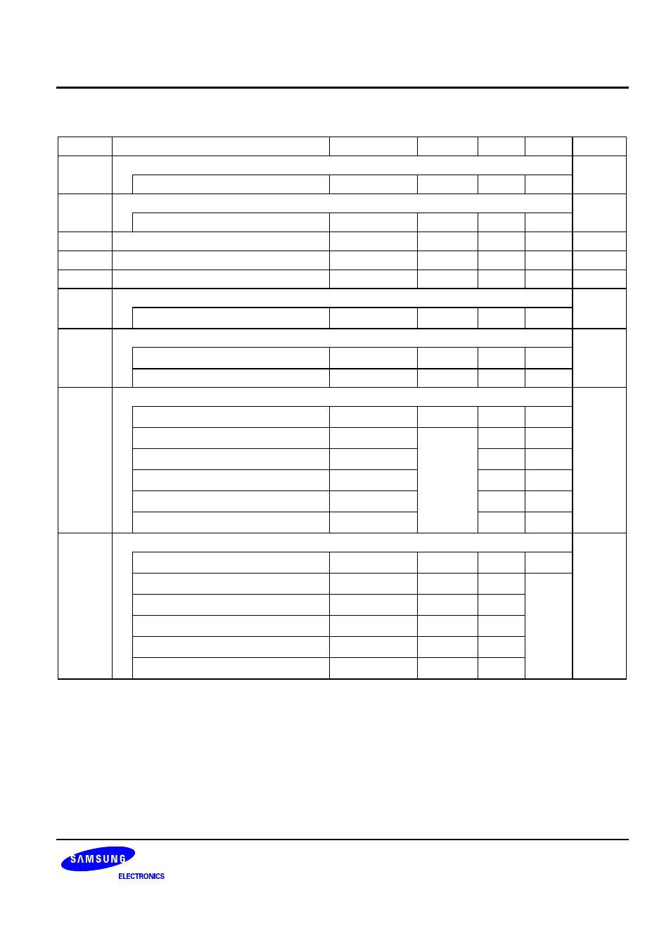
Normal I/O PAD DC Electrical Characteristics for I/O (V
DDOP
= 3.3V
±±±±
0.3V, T
A
= -40 to 85
°°°°
C)
Symbol Parameters
Condition
Min
Typ.
Max
Unit
High level input voltage
V
IH
LVCMOS
interface
2.0
V
Low level input voltage
V
IL
LVCMOS
interface
0.8
V
VT Switching
threshold
0.5V
DD
V
VT+
Schmitt trigger, positive-going threshold
CMOS
2.0
V
VT-
Schmitt trigger, negative-going threshold
CMOS
0.8
V
High level input current
I
IH
Input
buffer
V
IN
= V
DD
-10
10
µA
Low level input current
Input
buffer
V
IN
= V
SS
-10
10
I
IL
Input buffer with pull-up
-60
-33
-10
µA
High level output voltage
Type B4 to B12
I
OH
= - 1 µA
V
DD
-0.05
Type
B4
I
OH
= - 4 mA
Type
B6
I
OH
= - 6 mA
Type
B8
I
OH
= - 8 mA
Type
B10
I
OH
= -10 mA
V
OH
Type
B12
I
OH
= -12 mA
2.4
V
Low level output voltage
Type B4 to B12
I
OL
= 1 µA
0.05
Type
B4
I
OL
= 4 mA
Type
B6
I
OL
= 6 mA
Type
B8
I
OL
= 8 mA
Type
B10
I
OL
= 10 mA
V
OL
Type
B12
I
OL
= 12 mA
0.4
V
NOTES:
1. Type B6 means 6mA output driver cell.
2. Type B8 means 8mA output driver cell.
3. Type B12 means 12mA output driver cells.