Sdi special registers – Samsung S3C2440A User Manual
Page 440
MMC/SD/SDIO CONTROLLER
S3C2440A RISC MICROPROCESSOR
19-4
SDI SPECIAL REGISTERS
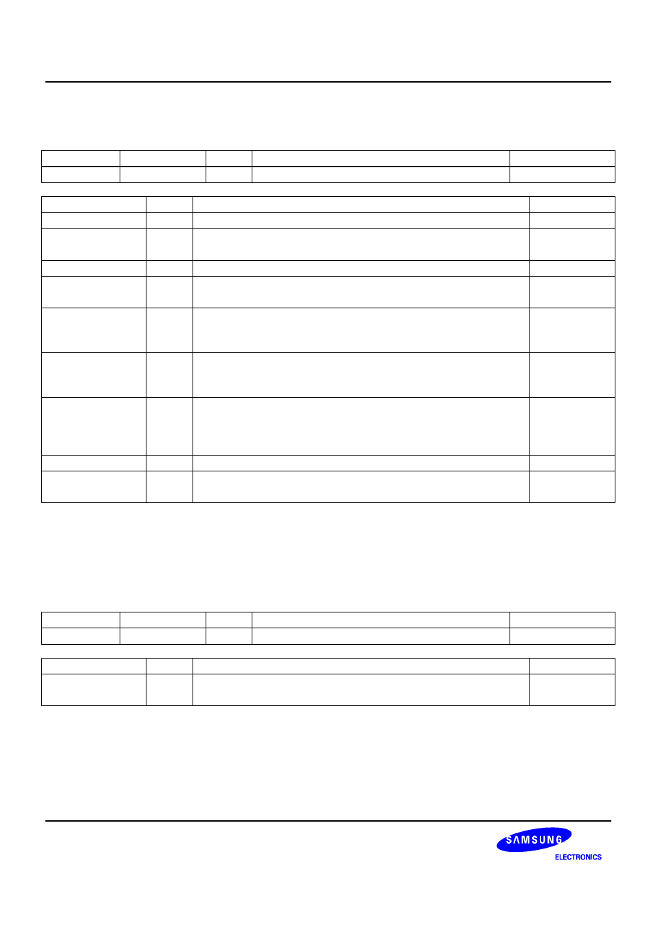
SDI Control Register(SDICON)
Register Address R/W
Description
Reset
Value
SDICON
0x5A000000
R/W
SDI Control Register
0x0
SDICON Bit
Description
Initial
Value
Reserved [31:9]
SDMMC Reset
(SDreset)
[8]
Reset whole sdmmc block. This bit is automatically cleared.
0 = normal mode, 1 = SDMMC reset
0
Reserved [7:6]
0
Clock Type
(CTYP)
[5]
Determines which clock type is used as SDCLK.
0 = SD type, 1 = MMC type
0
Byte Order
Type(ByteOrder)
[4]
Determines byte order type when you read(write) data from(to) sd
host FIFO with word boundary.
0 = Type A, 1 = Type B
0
Receive SDIO
Interrupt from card
(RcvIOInt)
[3]
Determines whether sd host receives SDIO Interrupt from the card
or not(for SDIO).
0 = ignore, 1 = receive SDIO Interrupt
0
Read Wait
Enable(RWaitEn)
[2]
Determines read wait request signal generate when sd host waits
the next block in multiple block read mode. This bit needs to delay
the next block to be transmitted from the card(for SDIO).
0 = disable(no generate), 1 = Read wait enable(use SDIO)
0
Reserved [1]
Clock Out Enable
(ENCLK)
[0]
Determines whether SDCLK Out enable or not
0 = disable(prescaler off), 1 = clock enable
0
* Byte Order Type
- Type A : (Access by Word) D[7:0]
→
D[15:8]
→
D[23:16]
→
D[31:24]
(Access by Halfword) D[7:0]
→
D[15:8]
- Type B : (Access by Word) D[31:24]
→
D[23:16]
→
D[15:8]
→
D[7:0]
(Access by Halfword) D[15:8]
→
D[7:0]
SDI Baud Rate Prescaler Register(SDIPRE)
Register Address R/W
Description
Reset
Value
SDIPRE
0x5A000004
R/W
SDI Buad Rate Prescaler Register
0x01
SDIPRE Bit
Description
Initial
Value
Prescaler Value
[7:0]
Determines SDI clock(SDCLK) rate as above equation.
Baud rate = PCLK / (Prescaler value + 1)
0x01
* Prescaler Value should be greater than zero.