Samsung S3C2440A User Manual
Page 490
S3C2440A RISC MICROPROCESSOR
CAMERA INTERFACE
23-12
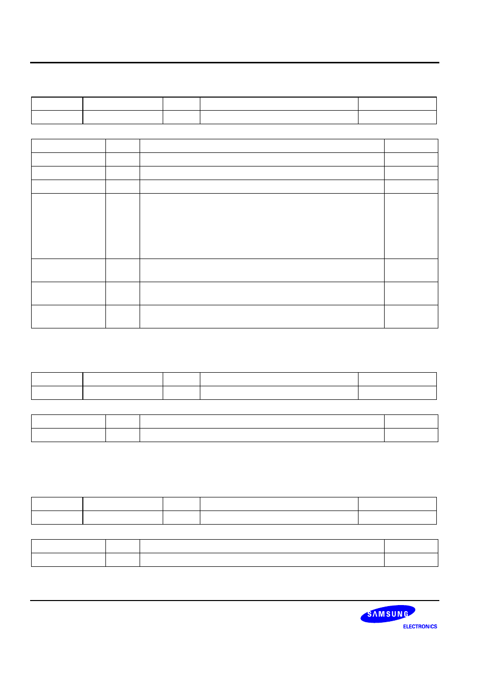
GLOBAL CONTROL REGISTER
Register Address R/W
Description
Reset
Value
CIGCTRL
0x4F000008
RW
Global Control Register
0
CIGCTRL Bit
Description
Initial
State
SwRst
[31]
Camera Interface Software Reset
0
CamRst
[30]
External Camera Processor Reset or Power Down
0
Reserved
[29]
This bit is reserved and the value must be 1.
1
TestPattern [28:27]
This register should be set only at ITU-T 601 8-bit mode. It is not
allowed with ITU-T 656 mode. (max. 1280 X 1024)
00 = External camera processor input (normal)
01 = Color bar test pattern
10 = Horizontal increment test pattern
11 = Vertical increment test pattern
0
InvPolCAMPCLK [26]
0 = Normal
1 = Inverse the polarity of CAMPCLK
0
InvPolCAMVSYNC [25]
0 = Normal
1 = Inverse the polarity of CAMVSYNC
0
InvPolCAMHREF [24]
0 = Normal
1 = Inverse the polarity of CAMHREF
0
Y1 START ADDRESS REGISTER
Register Address R/W
Description
Reset
Value
CICOYSA1 0x4F000018 RW Y
1
st
frame start address for codec DMA
0
CICOYSA1 Bit
Description
Initial
State
CICOYSA1 [31:0]
Y
1
st
frame start address for codec DMA
0
Note : Address of buffers must be multiple of 1024.
Y2 START ADDRESS REGISTER
Register Address R/W
Description
Reset
Value
CICOYSA2 0x4F00001C RW
Y
2
nd
frame start address for codec DMA
0
CICOYSA2 Bit
Description
Initial
State
CICOYSA2 [31:0]
Y
2
nd
frame start address for codec DMA
0