Samsung S3C2440A User Manual
Page 23
PRODUCT OVERVIEW
S3C2440A RISC MICROPROCESSOR
1-22
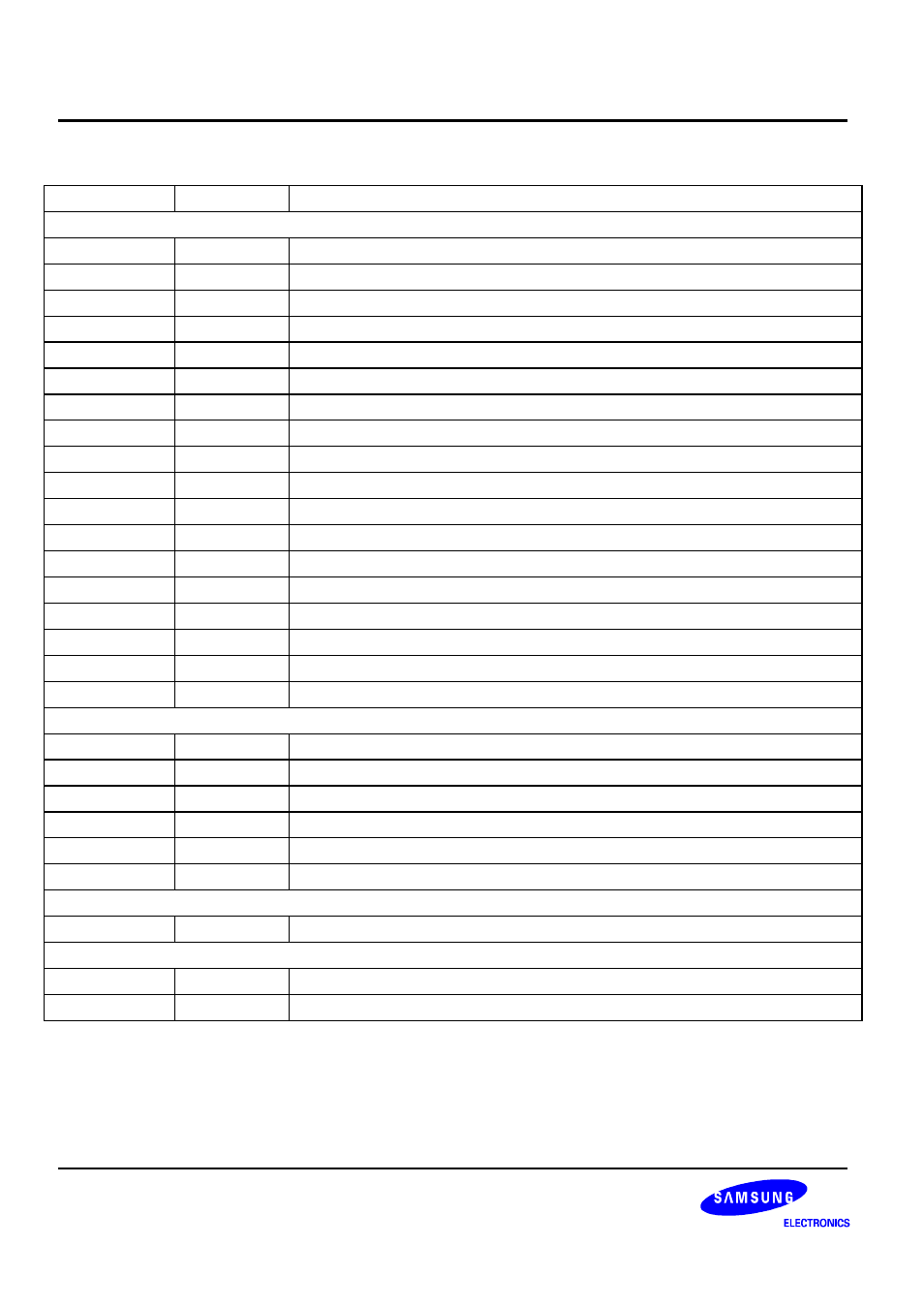
Table 1-3. S3C2440A Signal Descriptions (Sheet 2 of 6)
Signal Input/Output
Descriptions
LCD Control Unit
VD[23:0] O
STN/TFT/SEC TFT: LCD Data Bus
LCD_PWREN O
STN/TFT/SEC TFT: LCD panel power enable control signal
VCLK O
STN/TFT: LCD clock signal
VFRAME O
STN: LCD Frame signal
VLINE O
STN: LCD line signal
VM O
STN: VM alternates the polarity of the row and column voltage
VSYNC O
TFT: Vertical synchronous signal
HSYNC O
TFT: Horizontal synchronous signal
VDEN O
TFT: Data enable signal
LEND O
TFT: Line End signal
STV O
SEC TFT: SEC(Samsung Electronics Company) TFT LCD panel control signal
CPV O
SEC TFT: SEC(Samsung Electronics Company) TFT LCD panel control signal
LCD_HCLK O
SEC TFT: SEC(Samsung Electronics Company) TFT LCD panel control signal
TP O
SEC TFT: SEC(Samsung Electronics Company) TFT LCD panel control signal
STH O
SEC TFT: SEC(Samsung Electronics Company) TFT LCD panel control signal
LCD_LPCOE O
SEC TFT: Timing control signal for specific TFT LCD
LCD_LPCREV O
SEC TFT: Timing control signal for specific TFT LCD
LCD_LPCREVB O SEC TFT: Timing control signal for specific TFT LCD
CAMERA Interface
CAMRESET
O
Software Reset to the Camera
CAMCLKOUT
O
Master Clock to the Camera
CAMPCLK
I
Pixel clock from Camera
CAMHREF
I
Horizontal sync signal from Camera
CAMVSYNC
I
Vertical sync signal from Camera
CAMDATA[7:0]
I
Pixel data for YCbCr
Interrupt Control Unit
EINT[23:0]
I
External Interrupt request
DMA
nXDREQ[1:0]
I
External DMA request
nXDACK[1:0]
O
External DMA acknowledge