Samsung S3C2440A User Manual
Page 191
NAND FLASH CONTROLLER
S3C2440A RISC MICROPROCESSOR
6-6
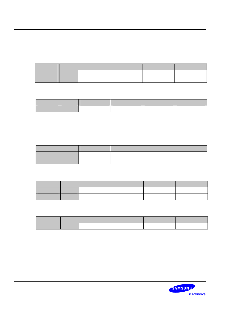
Data Register Configuration
1) 16-bit NAND Flash Memory Interface
A. Word
Access
Register
Endian
Bit [31:24]
Bit [23:16]
Bit [15:8]
Bit [7:0]
NFDATA
Little
2
nd
I/O[15:8]
2
nd
I/O[ 7:0]
1
st
I/O[15:8]
1
st
I/O[ 7:0]
NFDATA
Big
1
st
I/O[15:8]
1
st
I/O[ 7:0]
2
nd
I/O[15:8]
2
nd
I/O[ 7:0]
B. Half-word
Access
Register
Endian
Bit [31:24]
Bit [23:16]
Bit [15:8]
Bit [7:0]
NFDATA
Little/Big
Invalid value
Invalid value
1
st
I/O[15:8]
1
st
I/O[ 7:0]
2) 8-bit NAND Flash Memory Interface
A. Word
Access
Register
Endian
Bit [31:24]
Bit [23:16]
Bit [15:8]
Bit [7:0]
NFDATA
Little
4
th
I/O[ 7:0]
3
rd
I/O[ 7:0]
2
nd
I/O[ 7:0]
1
st
I/O[ 7:0]
NFDATA
Big
1
st
I/O[ 7:0]
2
nd
I/O[ 7:0]
3
rd
I/O[ 7:0]
4
th
I/O[ 7:0]
B. Half-word
Access
Register
Endian
Bit [31:24]
Bit [23:16]
Bit [15:8]
Bit [7:0]
NFDATA
Little
Invalid value
Invalid value
2
nd
I/O[ 7:0]
1
st
I/O[ 7:0]
NFDATA
Big
Invalid value
Invalid value
1
st
I/O[ 7:0]
2
nd
I/O[ 7:0]
C. Byte
Access
Register
Endian
Bit [31:24]
Bit [23:16]
Bit [15:8]
Bit [7:0]
NFDATA
Little/Big
Invalid value
Invalid value
Invalid value
1
st
I/O[ 7:0]
STEPPINGSTONE (4K-Byte SRAM)
The NAND Flash controller uses Steppingstone as the buffer on booting and also you can use this area for another
purpose.