Samsung S3C2440A User Manual
Page 478
SPI
S3C2440A RISC MICROPROCESSOR
22-8
The SPIMISO (MISO) and SPIMOSI (MOSI) data pins are used for transmitting and receiving serial data. When SPI
is configured as a master, SPIMISO (MISO) is the master data input line, SPIMOSI (MOSI) is the master data
output line, and SPICLK (SCK) is the clock output line. When SPI becomes a slave, these pins perform reverse
roles. In a multiple-master system, SPICLK (SCK) pins, SPIMOSI (MOSI) pins, and SPIMISO (MISO) pins are tied
to configure a group respectively. A master SPI can experience a multi master error, when other SPI device working
as a master selects the S3C2440A SPI as a slave. When this error is detected, the following actions are taken
immediately. But you must previously set SPPINn’s ENMUL bit if you want to detect this error.
1. The SPCONn's MSTR bit is forced to 0 to operate in slave mode.
2. The SPSTAn's MULF flag is set, and an SPI interrupt is generated.
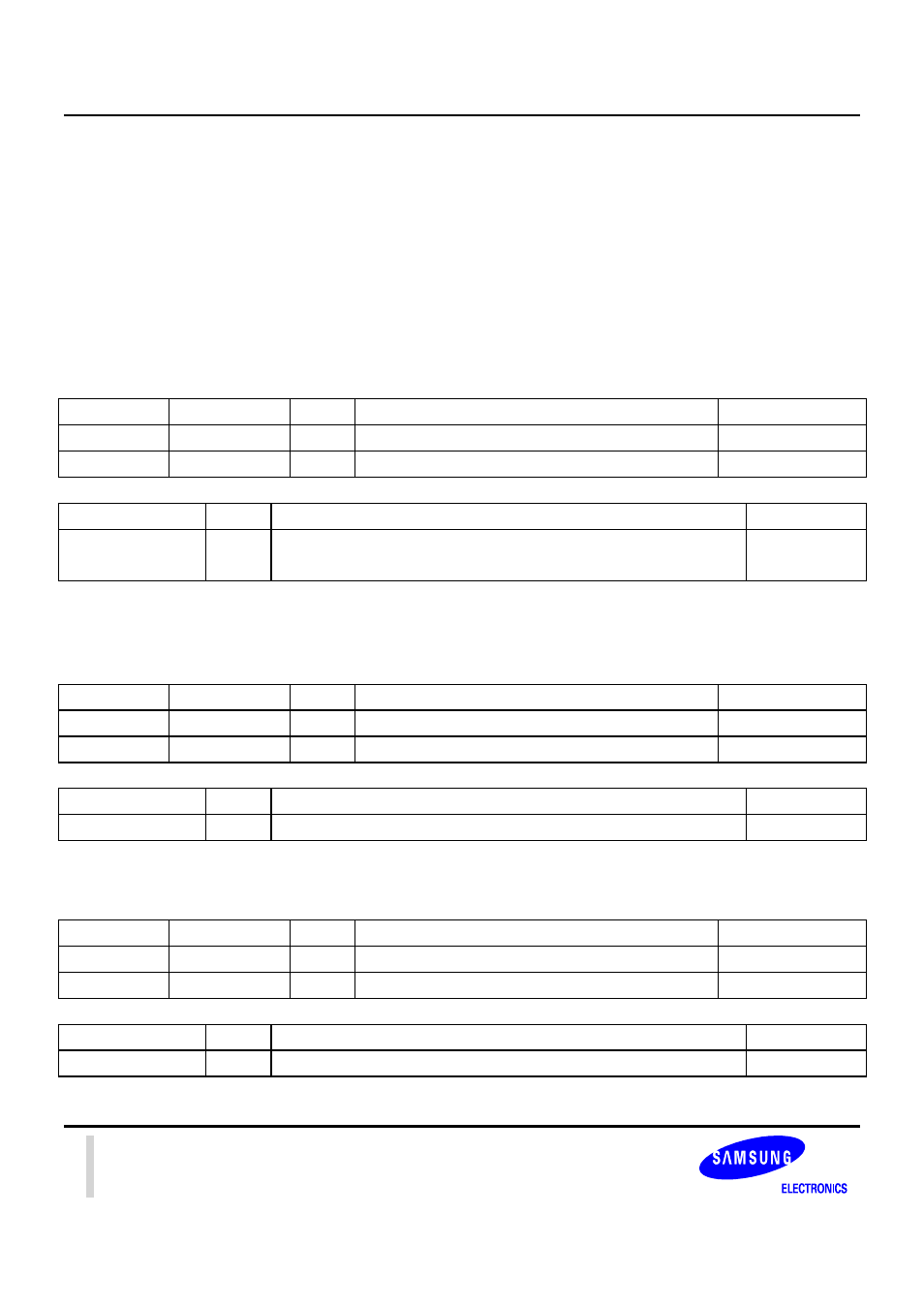
SPI BAUD RATE PRESCALER REGISTER
Register Address R/W
Description
Reset
Value
SPPRE0
0x5900000C
R/W
SPI cannel 0 baud rate prescaler register
0x00
SPPRE1
0x5900002C
R/W
SPI cannel 1 baud rate prescaler register
0x00
SPPREn Bit
Description
Initial
State
Prescaler Value
[7:0]
Determine SPI clock rate.
Baud rate = PCLK / 2 / (Prescaler value + 1)
0x00
NOTE
: Baud rate should be less than 25 MHz.
SPI TX DATA REGISTER
Register Address R/W
Description
Reset
Value
SPTDAT0
0x59000010
R/W
SPI channel 0 Tx data register
0x00
SPTDAT1
0x59000030
R/W
SPI channel 1 Tx data register
0x00
SPTDATn Bit
Description
Initial
State
Tx Data Register
[7:0]
This field contains the data to be transmitted over the SPI channel.
0x00
SPI RX DATA REGISTER
Register Address R/W
Description
Reset
Value
SPRDAT0
0x59000014
R
SPI channel 0 Rx data register
0xFF
SPRDAT1
0x59000034
R
SPI channel 1 Rx data register
0xFF
SPRDATn Bit
Description
Initial
State
Rx Data Register
[7:0]
This field contains the data to be received over the SPI channel.
0xFF