Samsung S3C2440A User Manual
Page 204
S3C2440A RISC MICROPROCESSOR NAND FLASH CONTROLLER
6-19
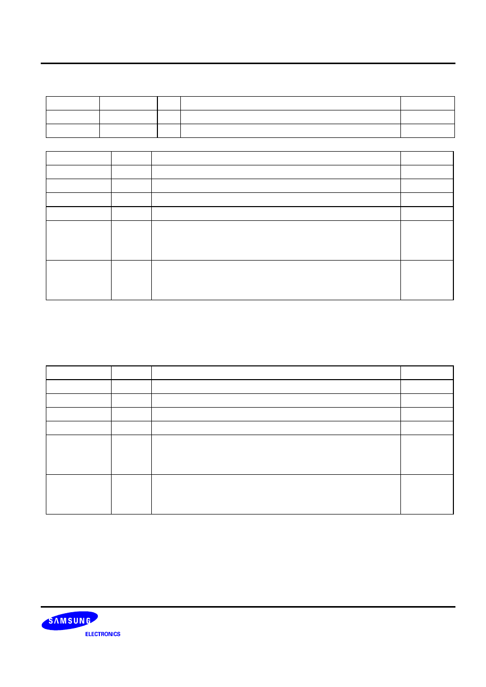
ECC0/1 STATUS REGISTER
Register
Address
R/W
Description
Reset Value
NFESTAT0
0x4E000024
R/W NAND Flash ECC Status register for I/O [7:0]
0x00000000
NFESTAT1
0x4E000028
R/W NAND Flash ECC Status register for I/O [15:8]
0x00000000
NFESTAT0 Bit
Description
Initial
State
SErrorDataNo
[24:21]
In spare area, Indicates which number data is error
00
SErrorBitNo
[20:18]
In spare area, Indicates which bit is error
000
MErrorDataNo
[17:7]
In main data area, Indicates which number data is error
0x00
MErrorBitNo
[6:4]
In main data area, Indicates which bit is error
000
SpareError
[3:2]
Indicates whether spare area bit fail error occurred
00: No Error
01: 1-bit error(correctable)
10: Multiple error
11: ECC area error
00
MainError
[1:0]
Indicates whether main data area bit fail error occurred
00: No Error
01: 1-bit error(correctable)
10: Multiple error
11: ECC area error
00
Note
The above value
s
are
only valid when
both
ECC register
and
ECC status register have valid value.
NFESTAT1 Bit
Description
Initial
State
SErrorDataNo
[24:21]
In spare area, Indicates which number data is error
00
SErrorBitNo
[20:18]
In spare area, Indicates which bit is error
000
MErrorDataNo
[17:7]
In main data area, Indicates which number data is error
0x00
MErrorBitNo
[6:4]
In main data area, Indicates which bit is error
000
SpareError
[3:2]
Indicates whether spare area bit fail error occurred
00: No Error
01: 1-bit error(correctable)
10: Multiple error
11: ECC area error
00
MainError
[1:0]
Indicates whether main data area bit fail error occurred
00: No Error
01: 1-bit error(correctable)
10: Multiple error
11: ECC area error
00
Note
The above value
s
are
only valid when
both
ECC register
and
ECC status register have valid value.