Timing diagram – Samsung S3C2440A User Manual
Page 481

S3C2440A RISC MICROPROCESSOR
CAMERA INTERFACE
23-3
TIMING DIAGRAM
jht}zuj
jht}zuj
jht}zuj
jht}zuj
j
j
j
j
j
jhtoylm
jhtoylm
jhtoylm
jhtoylm
jhtoylmG
jhtoylmG
jhtoylmG
jhtoylmG
OXoP
OXoP
OXoP
OXoP
jhtwjsr
jhtwjsr
jhtwjsr
jhtwjsr
jhtkh{h
jhtkh{h
jhtkh{h
jhtkh{h
^aW
^aW
^aW
^aW
}G
}G
}G
}G
o¡G
o¡G
o¡G
o¡G
XG
XG
XG
XG
_TG
_TG
_TG
_TG
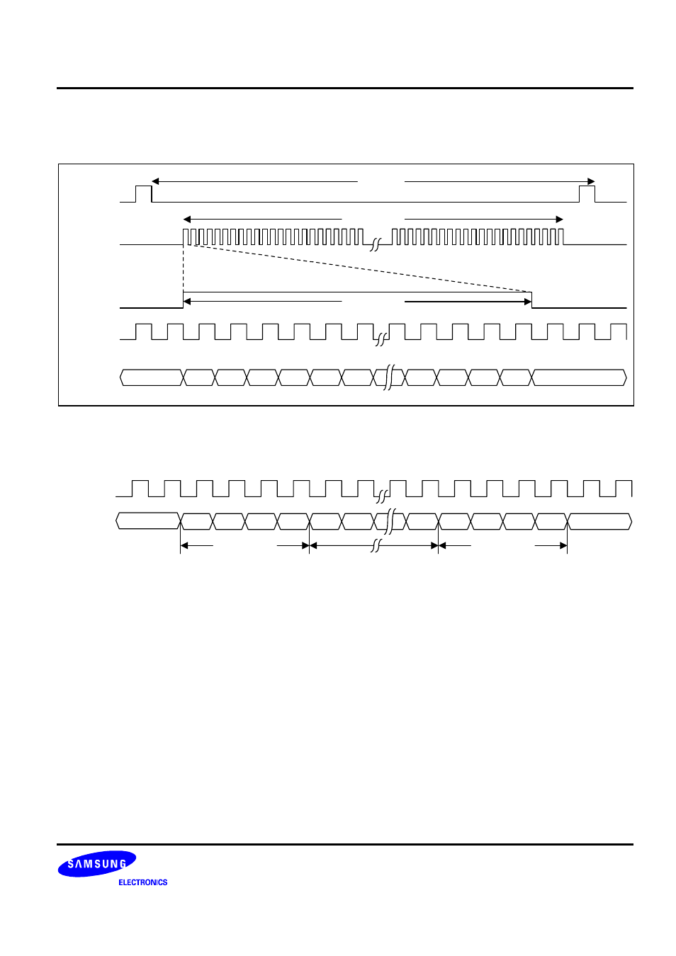
Figure 23-2 ITU-R BT 601 Input Timing Diagram
jhtwjsr
jhtwjsr
jhtwjsr
jhtwjsr
jhtkh{h
jhtkh{h
jhtkh{h
jhtkh{h
^aW
^aW
^aW
^aW
j
mm
mm
mm
mm
WW
WW
WW
WW
WW
WW
WW
WW
j
mm
mm
mm
mm
WW
WW
WW
WW
WW
WW
WW
WW
}G
}G
}G
}G
G
G
G
G
wG
wG
wG
wG
}G
}G
}G
}G
G
G
G
G
Figure 23-3 ITU-R BT 656 Input Timing Diagram
There are two timing reference signals in ITU-R BT 656 format, one is at the beginning of each video data block
(start of active video, SAV) and other is at the end of each video data block (end of active video, EAV) as shown in
Figure 23-3 and Table 23-2.
