Function description – Samsung S3C2440A User Manual
Page 168
S3C2440A RISC MICROPROCESSOR
MEMORY CONTROLLER
DEC.13, 2002
5-3
FUNCTION DESCRIPTION
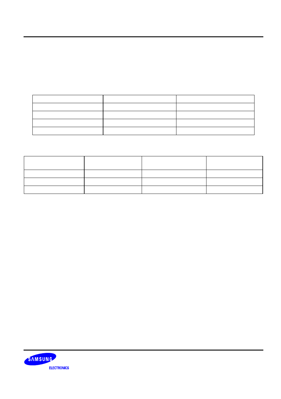
BANK0 BUS WIDTH
The data bus of BANK0 (nGCS0) should be configured with a width as one of 16-bit and 32-bit ones. Because the
BANK0 works as the booting ROM bank (map to 0x0000_0000), the bus width of BANK0 should be determined
before the first ROM access, which will depend on the logic level of OM[1:0] at Reset.
OM1 (Operating Mode 1)
OM0 (Operating Mode 0)
Booting ROM Data width
0
0
Nand Flash Mode
0 1 16-bit
1 0 32-bit
1 1
Test
Mode
MEMORY (SROM/SDRAM) ADDRESS PIN CONNECTIONS
MEMORY ADDR. PIN
S3C2440A ADDR.
@ 8-bit DATA BUS
S3C2440A ADDR.
@ 16-bit DATA BUS
S3C2440A ADDR.
@ 32-bit DATA BUS
A0 A0 A1 A2
A1 A1 A2 A3
. . .
. . .
. . .
. . .
See also other documents in the category Samsung Notebooks:
- NC10 (12 pages)
- GT-P7300 (133 pages)
- M6000 (130 pages)
- M60 (201 pages)
- P55 (172 pages)
- Tablet (44 pages)
- Q45c (199 pages)
- Galaxy Tab 8.9 (188 pages)
- X22 (197 pages)
- Q46 (194 pages)
- GT-P7100 (108 pages)
- R71 (196 pages)
- Q71 (191 pages)
- M55 (161 pages)
- GT-P6210 (200 pages)
- V1.3.0 (26 pages)
- Q35 (157 pages)
- 8.9 (176 pages)
- X65 (195 pages)
- Galaxy Tab A3LSGHI987 (146 pages)
- GALAXY Tab SGH-I987 (149 pages)
- Q30 (127 pages)
- NP270E5V (27 pages)
- NP670Z5E (157 pages)
- NP275E5E (135 pages)
- NP270E5GI (134 pages)
- NP535U3C (154 pages)
- NP370R5E (133 pages)
- XE500T1C (122 pages)
- XE500T1C (117 pages)
- NP270E5UE (27 pages)
- NP930X5J-S01US (115 pages)
- NP930X5J-S01US (149 pages)
- NP900X3D-A03US (138 pages)
- NP900X4D-A03US (129 pages)
- NP470R5E-K01UB (120 pages)
- NP470R5E-K01UB (126 pages)
- NP470R5E-K01UB (125 pages)
- NP700Z3C-S01US (156 pages)
- NP355V4C-A01VE (140 pages)
- NP940X3G-S01US (149 pages)
- NP940X3G-S01US (147 pages)
- NP915S3G-K02US (145 pages)
- NP915S3G-K02US (118 pages)