Samsung S3C2440A User Manual
Page 22
S3C2440A RISC MICROPROCESSOR
PRODUCT OVERVIEW
1-21
SIGNAL DESCRIPTIONS
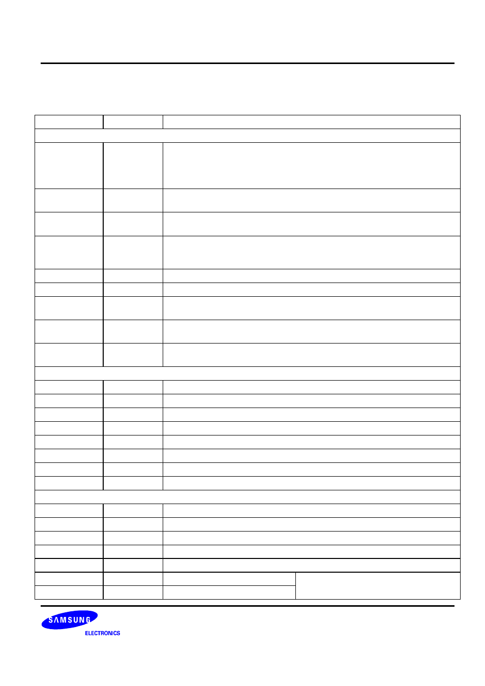
Table 1-3. S3C2440A Signal Descriptions (Sheet 1 of 6)
Signal Input/Output
Descriptions
Bus Controller
OM[1:0]
I
OM[1:0] sets S3C2440A in the TEST mode, which is used only at fabrication.
Also, it determines the bus width of nGCS0. The pull-up/down resistor
determines the logic level during RESET cycle.
00:Nand-boot
01:16-bit 10:32-bit 11:Test
mode
ADDR[26:0]
O
ADDR[26:0] (Address Bus) outputs the memory address of the corresponding
bank .
DATA[31:0]
IO
DATA[31:0] (Data Bus) inputs data during memory read and outputs data during
memory write. The bus width is programmable among 8/16/32-bit.
nGCS[7:0]
O
nGCS[7:0] (General Chip Select) are activated when the address of a memory is
within the address region of each bank. The number of access cycles and the
bank size can be programmed.
nWE
O
nWE (Write Enable) indicates that the current bus cycle is a write cycle.
nOE
O
nOE (Output Enable) indicates that the current bus cycle is a read cycle.
nXBREQ
I
nXBREQ (Bus Hold Request) allows another bus master to request control of the
local bus. BACK active indicates that bus control has been granted.
nXBACK
O
nXBACK (Bus Hold Acknowledge) indicates that the S3C2440A has surrendered
control of the local bus to another bus master.
nWAIT
I
nWAIT requests to prolong a current bus cycle. As long as nWAIT is L, the
current bus cycle cannot be completed.
SDRAM/SRAM
nSRAS
O
SDRAM Row Address Strobe
nSCAS
O
SDRAM Column Address Strobe
nSCS[1:0]
O
SDRAM Chip Select
DQM[3:0]
O
SDRAM Data Mask
SCLK[1:0] O
SDRAM
Clock
SCKE
O
SDRAM Clock Enable
nBE[3:0]
O
Upper Byte/Lower Byte Enable(In case of 16-bit SRAM)
nWBE[3:0]
O
Write Byte Enable
NAND Flash
CLE
O
Command Latch Enable
ALE
O
Address Latch Enable
nFCE
O
Nand Flash Chip Enable
nFRE
O
Nand Flash Read Enable
nFWE
O
Nand Flash Write Enable
NCON
I
Nand Flash Configuration
FRnB
I
Nand Flash Ready/Busy
* If NAND flash controller isn’t used, it has
to be pull-up. (3.3V)