Oki B4100 User Manual
Page 490
40055101TH Rev.4
490 /
A3.11 MEMO (memory) Circuit Diagram for OKIFAX 5000 Series (option)
By mounting this optional memory board (MEM/MEM-2), it can be used for the expansion memory.
1.
Block diagram
Figure A3.11.1 shows a related signal of memory board.
Memory board circuit consists of the following block.
1)
512 kbyte MOS Dynamic RAM x 4 (IC3 to IC6).
Used as follows:
•
Picture memory for the ECM send/receive modes.
•
Picture memory for the memory transmission mode.
•
Picture memory for the retransmission data.
•
Picture memory for the reception in memory
2)
Memory capacity
•
1 Mbyte memory board can be added for OKIFAX 5200/5300.
•
One of 1 Mbyte memory board can be added for OKIFAX 5000 series.
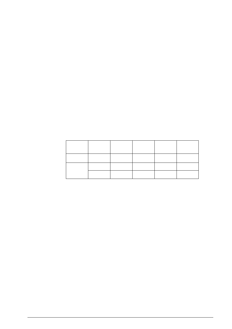
The relationship between memory capacity and mounted boards are shown in the following
table.
Note: Back-up time on electrical interruption; Min. one hour for OKIFAX 5000 series.
Equipment
OKIFAX
5200/5300
Memory
Capacity
1 Mbyte
Mounted
Mounted
Not mounted
Not mounted
IC3
IC4
IC5
IC6
OKIFAX
5500/5600
1 Mbyte
2 Mbyte
Mounted
Mounted
Mounted
Mounted
Not mounted
Mounted
Not mounted
Mounted