Oki B4100 User Manual
Page 406
40055101TH Rev.4
406 /
A3.2.4
M17 Circuit Diagram (Page 4/17)
1.
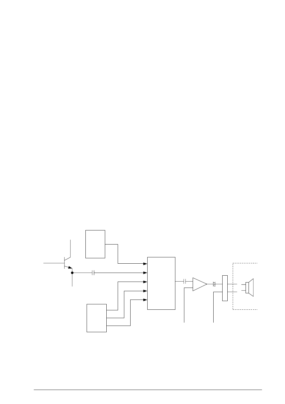
Block diagram
The audio monitor circuit on page 4/17 that consists of IC11 (analog switch IC) and IC5 (ampli-
fier) generates the following audio monitor.
•
Line monitoring
•
Buzzer signals
Figure A3.2.4 shows the block diagram of audio monitor circuit.
2.
Function
1)
Line monitoring
Send and receive signals are input from the transformer on the NCU board to this circuit as
RM signal and the signal power is input to the IC11. The IC11 adjusts the monitor volume
by MONC0, MONC1 and MONC2 signal under the control of IOGA3. Output (high and
low) from IC11 passes through the amplifier and fed to the speaker as a SP signal.
•
MONC0/MONC1/MONC2 signal :
Volume control signal.
Note: In case of transmission mode, the monitor will be available during dialing, but the
monitor will be switched off automatically after the elapse of specified time (about
5 sec).
2)
Buzzer control
Alarm and other signals (key touch etc.) are input from CPU to this circuit as BZ signal.
The various buzzer signals are sounded under the control of CPU.
Figure A3.2.4 Block Diagram of Audio Monitor Circuit
IC11
IC2
IOGA
CPU
RM
Analog
switch
IC5
Amplifier
CN8
1
2
Speaker
BZ
MONC0
MONC1
MONC2
0V
0VA
+5 V
0VA
from modem
TR1