Oki B4100 User Manual
Page 391

40055101TH Rev.4
391 /
1.
Block diagram
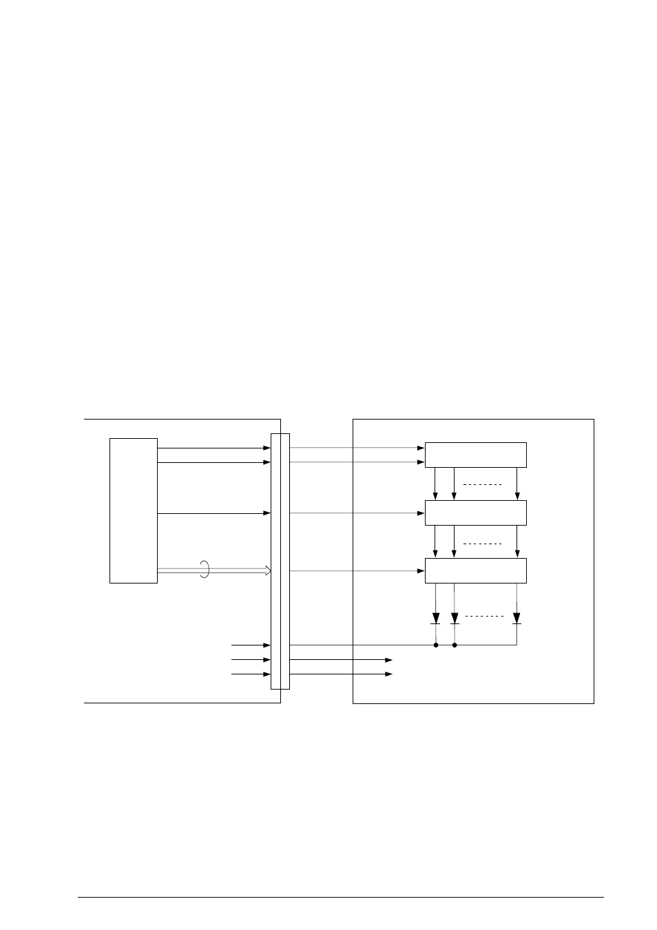
The circuit diagram shown on page 7/12 consists of connector CN14 that provides an interface
between R44 board and LED print head.
Figure A3.1.7 shows the related signals and block diagram of LED print head.
2.
Function
Data of 1664 LEDs on the LED print head is loaded into the shift registers by the HCLCK (1.0
MHz) signal. After the 1664 bit (208 mm) data is loaded in the shift registers, it is then loaded in
the latch circuit by the HLATCH signal. The turning -on and off of the LEDs are controlled by
STRB1-N to STRB4-N signals.
LED head interface signals output from IOGA1
•
HDATA 0
: Print data i.e., data to be printed
•
HCLCK
: Transfer clock for print data (4.0 MHz)
•
HLATCH
: Latch signal for print data
•
STRB1-N to STRB4-N : LED head strobe signals
A3.1.8
R44 Circuit Diagram (Page 8/12)
Shift register
Latch
Strobe
CN14
8
6
9
10, 11, 12, 13
1, 2
3, 4
5, 14
+5 V
0 V
LED
1664 bits (208 mm)
LED print head
R44
HCLCK (1.0 MHz)
HDATA 0
HLATCH
STRB1-N to STRB4-N
0 VP
+5 V
0 V
IOGA
IC2
Figure A3.1.7 Related Signals and Block Diagram of LED Head
