Oki B4100 User Manual
Page 404
40055101TH Rev.4
404 /
A3.2.2
M17 Circuit Diagram (Page 2/17)
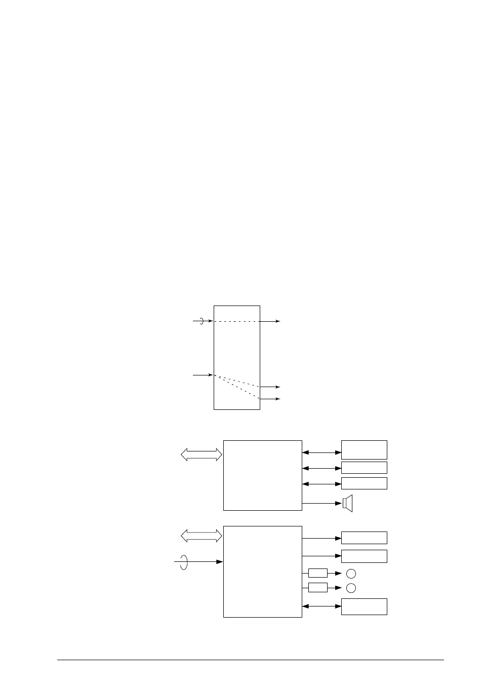
1.
Block diagram
The circuit diagram shown on page 2/17 consists of an input/output gate array IC2 (IOGA3).
Figure A3.2.2 shows the related signals of IOGA3.
2.
Functions
IOGA3 is newly developed LSI for scanning and printing control of OKIFAX 5000 series.
IOGA3 contains the following functions:
•
Strobe signals control for LED head
•
Smoothing control for printing data
•
Interface of the peripheral LSI and CPU
3.
Others
1)
The route to transfer print data to the LED head is follows:
•
Data bus route: RX, Memory, Report mode, etc.
2)
System clock (CLK) is divided by IOGA3 and these divided clocks are transferred to the
IEXSEED (IC20), LED head and 2’nd tray.
IOGA3
Data bus
HDATA
System clock
(20.000 MHz)
HCLCK (6.67 MHz/10MHz): to LED head
OPCLK-N (156.25 kHz): to 2'nd tray
AD00
to
AD15
Figure A3.2.2 Related Signals of IOGA
Data/address bus
Printer control
OST-EX
Buffer 640 bytes
Decompressed
(RLE, TIFF, ACC32)
200-300/300-200 con-
verter
High-voltage control
smoothing
Various sensor
M
D-motor
2/2
LED head
Power supply
unit
Fan
Data/address bus
Peripheral control
1284 control
CS generation
I/O port
1/2
Bi-Centro
I/F
CTR
OPE unit
2nd tray
Speaker
DRV
M
R-motor
DRV