Oki B4100 User Manual
Page 384

40055101TH Rev.4
384 /
+5 V
IC1
X1
20 MHz
PWRDY-N
20 MHz
Initial Reset Circuit
Address bus
RES
XTAL
EXTAL
CPU
Port C
Data/Address bus
Port A
Port B
CK
(PC1/PC2)
M
D-motor
Clutch
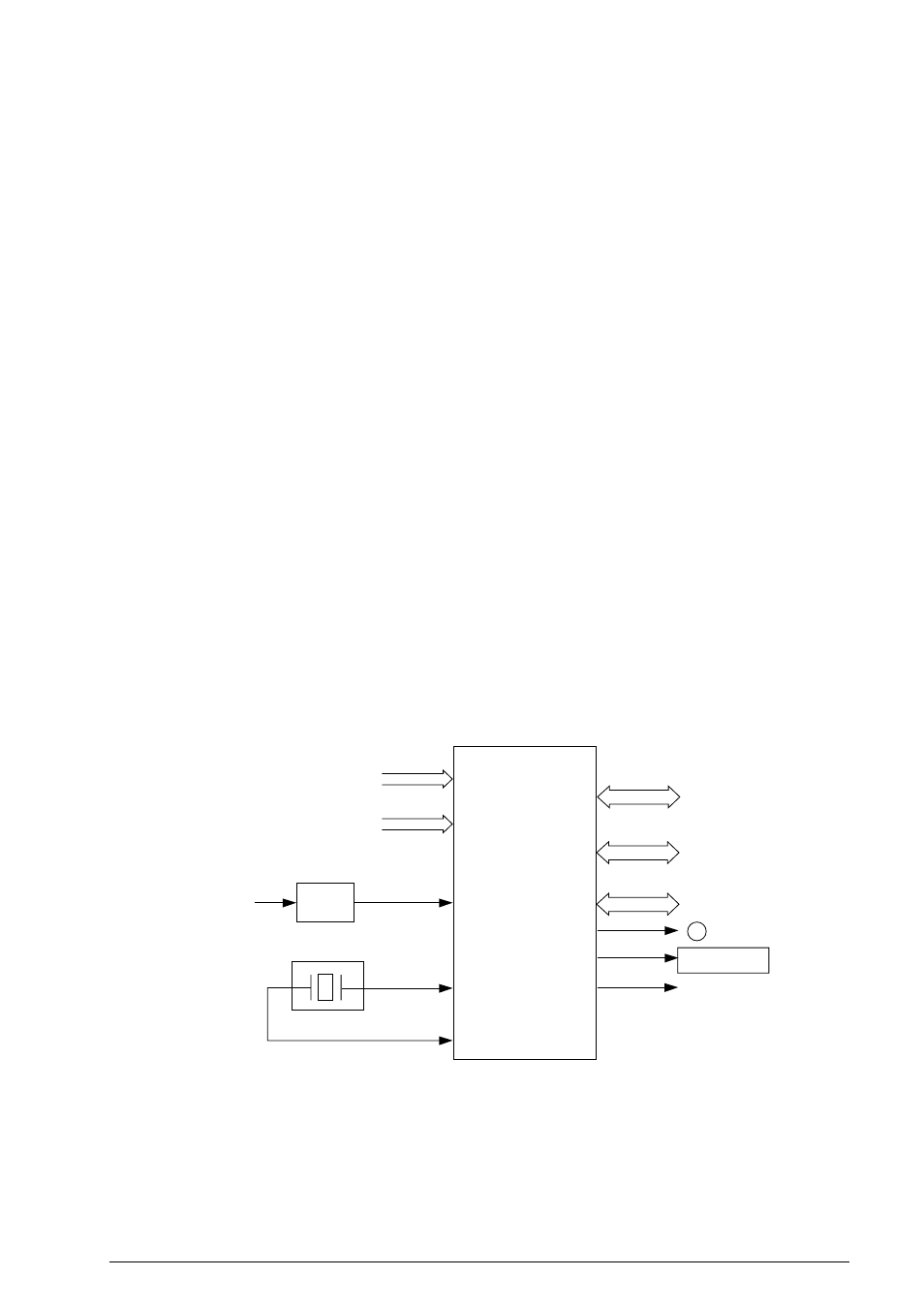
Figure A3.1.1 Related Signals of CPU
A3.1
R44 Circuit Diagram (for OKIOFFICE 44/OKIFAX 4100)
A3.1.1
R44 Circuit Diagram (Page 1/12)
1.
Block diagram
The circuit diagram shown on page 1/12 consists of the CPU, crystal oscillator circuit and reset
signal generator.
Figure A3.1.1 shows the block diagram of CPU and the peripheral circuits.
2.
Function
1)
Crystal oscillator circuit
X1 is a 20 MHz crystal ocillator. The output wave is fed to the CPU through pin 73 and 74.
CLK (20 MHz) signal output from pin 71 is used as the system clock and output to IC2
(IOGA3: input/output gate array).
2)
CPU
CPU controls the following functions in addition to the basic processor.
•
DMA (Direct Memory Access) control
•
Interrupt procedure control
•
A/D converter
•
Bus state control
•
Programmable pattern control
•
16 bit integrated timer pulse unit (ITU)
•
Timing pattern control (TPC)
•
Serial communication interface (SCI)
