Oki B4100 User Manual
Page 389

40055101TH Rev.4
389 /
1.
Block diagram
The circuit diagram shown on page 5/12 consists of the following functions:
•
IC6 (A/D converter)
•
30 V/24 V conversion circuit
•
Connector CN5 that provides an interface between R44 board and CIS (contact image sensor).
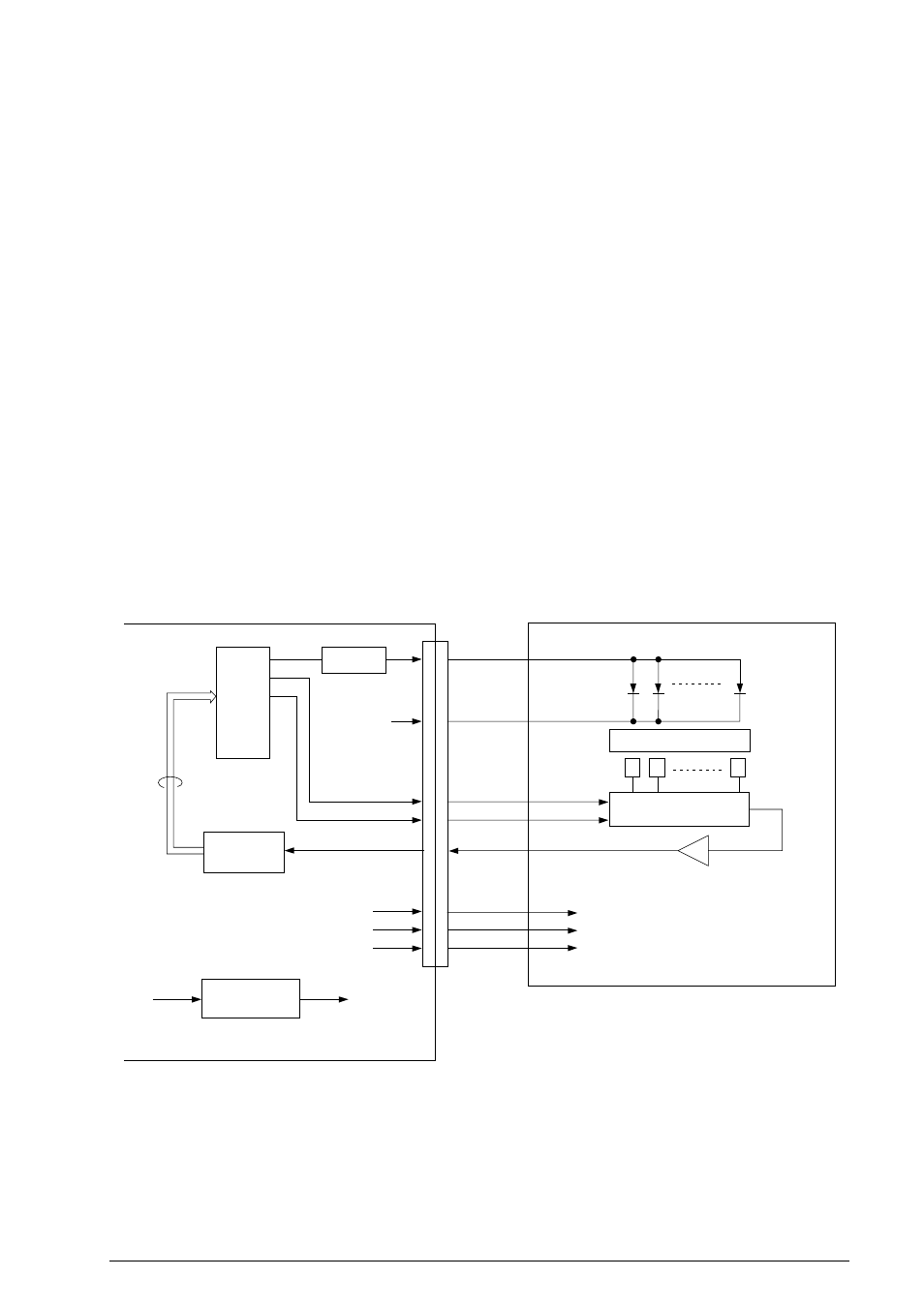
Figure A3.1.5 shows the related signals and block diagram of CIS.
2.
Function
One-line picture data is read in the sequence from the scanning unit (CIS) as SIG signal (analog
data) to A/D converter (analog/digital converter) of IC6. After conversion from analog data to 6-
bit digital signal (SDATA0 - SDATA5) under the control of IC6, this picture data is sent to
IOGA3 (input/output gate array). Here, the picture data undergoes various kinds of picture
processings.
Sensor interface signal output from IOGA3
•
LEDON :
LED on/off control signal
•
SNSCLK :
Scanning sensor drive clock (714.286 kHz)
•
MISP
:
Scanning synchronous signal (5 msec)
•
ADCLK :
Sampling clock for A/D converter (714.286 kHz)
A3.1.6
R44 Circuit Diagram (Page 6/12)
Shift register & analog switches
CN5
10
3
4
2, 5, 7
-8 V
0 VA
CIS (contact image sensor)
R44
VLED
+5 V
-8 V
0 VA
LEDs array
Rod lens array
sensor
1728 bit (216 mm)
+5 V
9
6
8
1
VLED (+24V)
GLED
MISP
DCK
SIG
GLED
MISP
DCK (714.286 kHz)
SIG
A/D converter
Amplifier
TR9/TR10
Transistor
LEDON
IOGA
IC2
SDATA0 - SDATA5
IC6
30 V/24 V conversion
circuit
30V
24 V
Figure A3.1.5 Related Signals and Block Diagram of CIS (contact image sensor)
