Oki B4100 User Manual
Page 409
40055101TH Rev.4
409 /
A3.2.7
M17 Circuit Diagram (Page 7/17, 8/17, 17/17)
1.
Block diagram
The circuit diagram shown on page 8/17 consists of connector CN15 that provides an interface
between M17 board and the Modem board (28.8 kbps).
The circuit diagram shown on page 7/17 consists of Modem (14.4kbps).
The circuit diagram shown on page 17/7 consists of Modem (V34 modem or S34).
Modem consists the following functions:
•
Modulation/demodulation
Modulation type:
1)
ITU-T Rec. V34 (28800 bps) for G3 picture data: OKIFAX 5500/5600
2)
ITU-T Rec. V17 (14400/12000/9600/7200 bps) for G3 picture data.
3)
ITU-T Rec. V33 (14400/12000 bps) for G3 picture data.
4)
ITU-T Rec. V29 (9600/7200 bps) for G3 picture data.
5)
ITU-T Rec. V27 ter (4800/2400 bps) for G3 picture data.
6)
ITU-T Rec. V21 channel 2 (300bps) for binary signals defined in ITU-T Rec. T.30.
•
Automatic adaptive equalizer for G3 receive data with 300 bps data excluded.
•
Generation of signal tones
•
PB tone (multi-frequency tone) generation
•
Detection of single tones
•
D/A converter for send data (TX)
•
A/D converter for receive data (RX)
•
Amplitude equalizer for RX
•
Selectable attenuation for TX
•
Automatic gain control
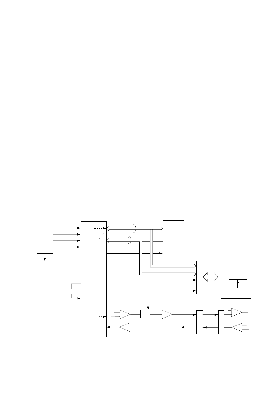
Figure A3.2.8 shows the related signals of Modem.
Figure A3.2.8 Related Signals of Modem
X'tal
X'tal
CPU
Modem
14.4 kbps
AD0 to AD7
A1 to A7
MDINT1-N
CN6
CN15
NCU
29.4912 MHz
M17
IC8
S
R
IOGA3
CS1-N
MDRST-N
MDMRD-N
MDMWR-N
IC12
IC12
IC29
IC30
SW
7
1
1
R
TXL
OKIFAX 5500/5600
Modem
28.8 Kbps
(V34)
1
1
CN200
CN3
18/18