Oki B4100 User Manual
Page 407

40055101TH Rev.4
407 /
A3.2.5
M17 Circuit Diagram (Page 5/17)
1.
Block diagram
The circuit diagram shown on page 5/17 consists of the following function:
•
IC6 (A/D converter) and amplifier
•
30 V/24 V conversion circuit
•
Connector CN10 that provides an interface between M17 board and CIS (contact
image sensor).
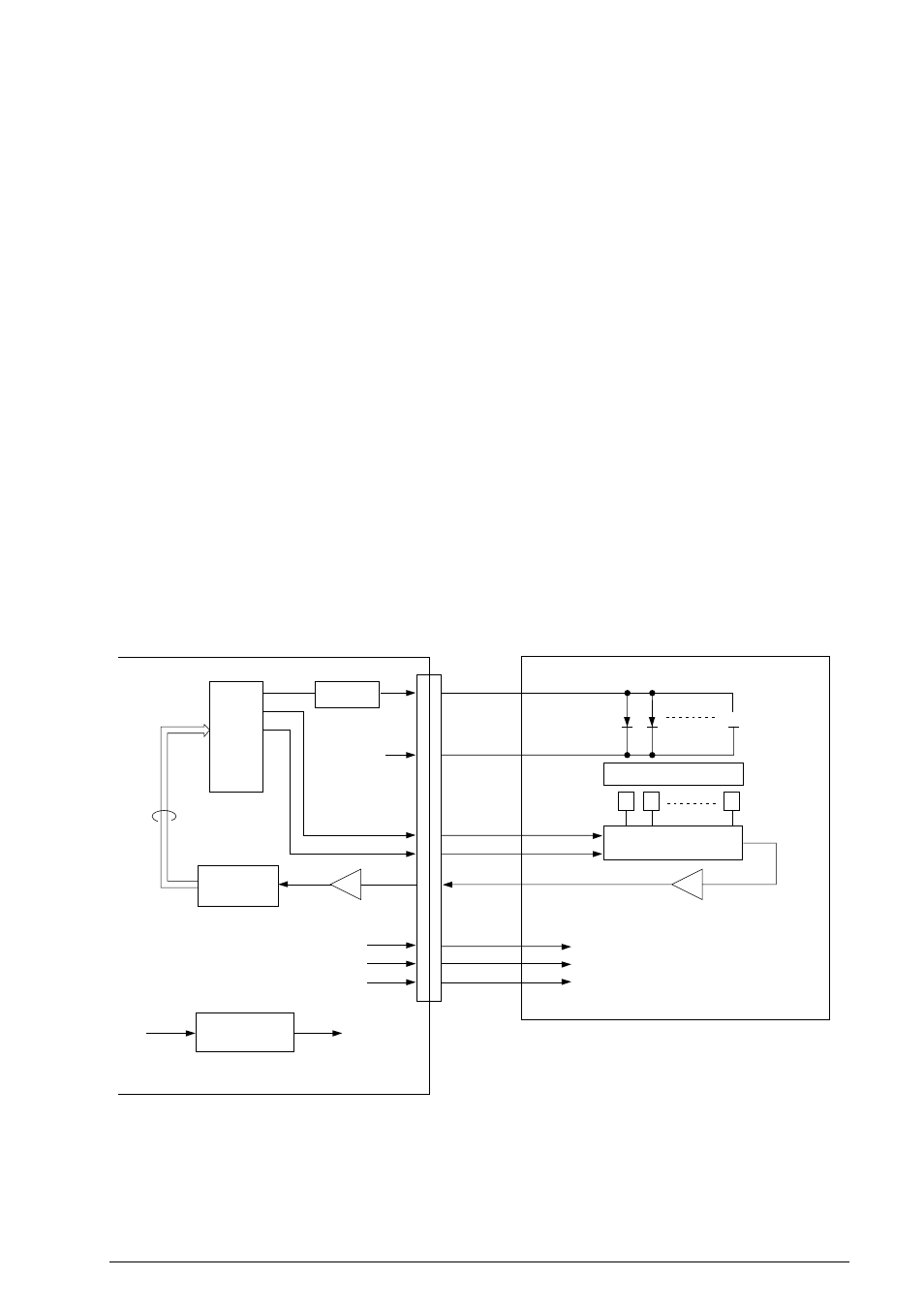
Figure A3.2.5 shows the related signals and block diagram of CIS.
2.
Function
One-line picture data is read in the sequence from the scanning unit (CIS) as SIG signal (analog
data) to A/D converter (analog/digital converter) of IC6 via amplifier. After conversion from
analog data to 6-bit digital signal (SDT2 - SDT7) under the control of IC6, the picture data is sent
to EXSEED (scanning control LSI) of IC20. Here, the picture data undergoes various kinds of
picture processings.
Sensor interface signal output from EXSEED.
•
LEDON: LED on/off control signal
•
PDCK : Scanning sensor drive clock (1.25MHz for ODA/833KHz for INT'L)
•
MISP
: Scanning synchronous signal (2.5 msec)
•
ADCLK: Sampling clock for A/D converter (1.25MHz for ODA/833KHz for INT'L)
Shift register & analog switches
CN10
10
3
4
2, 5, 7
-8 V
0 VA
CIS (contact image sensor)
M17
VLED
+5 V
-8 V
0 VA
LEDs array
Rod lens array
sensor
1728 bit (216 mm)
+5 V
9
6
8
1
VLED (+24 V)
GLED
MISP
DCK
SIG
GLED
MISP
PDCK (1.25MHz/833KHz)
SIG
Amplifier
A/D converter
Amplifier
TR9/TR10
Transistor
LEDON
EXSEED
IC20
SDT2 - SDT7
IC6
30 V/24 V conversion
circuit
30 V
24 V
Figure A3.2.5 Related Signals and Block Diagram of CIS (contact image sensor)
