Portg - port g data register, Ddrg - port g data direction register, Ping - port g input pins address – Rainbow Electronics ATmega3290P_V User Manual
Page 88: Porth - port h data register(1), Ddrh - port h data direction register(1), Pinh - port h input pins address(1), Portj - port j data register(1), Ddrj - port j data direction register(1), Pinj - port j input pins address(1), Ddrh – port h data direction regist er
88
ATmega329/3210/649/6410
2552H–AVR–11/06
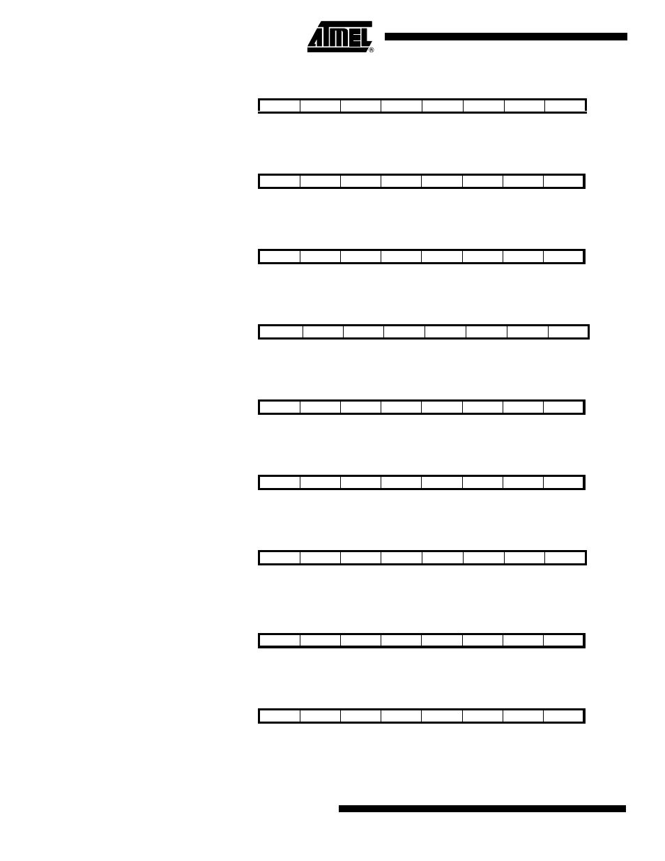
PORTG – Port G Data Register
DDRG – Port G Data Direction
Register
PING – Port G Input Pins
Address
PORTH – Port H Data
Register
DDRH – Port H Data Direction
Register
PINH – Port H Input Pins
Address
PORTJ – Port J Data
Register
DDRJ – Port J Data Direction
Register
PINJ – Port J Input Pins
Address
Note:
1. Register only available in ATmega3290/6490.
Bit
7
6
5
4
3
2
1
0
–
–
–
PORTG4
PORTG3
PORTG2
PORTG1
PORTG0
PORTG
Read/Write
R
R
R
R/W
R/W
R/W
R/W
R/W
Initial Value
0
0
0
0
0
0
0
0
Bit
7
6
5
4
3
2
1
0
–
–
–
DDG4
DDG3
DDG2
DDG1
DDG0
DDRG
Read/Write
R
R
R
R/W
R/W
R/W
R/W
R/W
Initial Value
0
0
0
0
0
0
0
0
Bit
7
6
5
4
3
2
1
0
–
–
PING5
PING4
PING3
PING2
PING1
PING0
PING
Read/Write
R
R
R
R/W
R/W
R/W
R/W
R/W
Initial Value
0
0
0
N/A
N/A
N/A
N/A
N/A
Bit
7
6
5
4
3
2
1
0
PORTH7
PORTH6
PORTH5
PORTH4
PORTH3
PORTH2
PORTH1
PORTH0
PORTH
Read/Write
R/W
R/W
R/W
R/W
R/W
R/W
R/W
R/W
Initial Value
0
0
0
0
0
0
0
0
Bit
7
6
5
4
3
2
1
0
DDH7
DDH6
DDH5
DDH4
DDH3
DDH2
DDH1
DDH0
DDRH
Read/Write
R/W
R/W
R/W
R/W
R/W
R/W
R/W
R/W
Initial Value
0
0
0
0
0
0
0
0
Bit
7
6
5
4
3
2
1
0
PINH7
PINH6
PINH5
PINH4
PINH3
PINH2
PINH1
PINH0
PINH
Read/Write
R/W
R/W
R/W
R/W
R/W
R/W
R/W
R/W
Initial Value
N/A
N/A
N/A
N/A
N/A
N/A
N/A
N/A
Bit
7
6
5
4
3
2
1
0
–
PORTJ6
PORTJ5
PORTJ4
PORTJ3
PORTJ2
PORTJ1
PORTJ0
PORTJ
Read/Write
R
R/W
R/W
R/W
R/W
R/W
R/W
R/W
Initial Value
0
0
0
0
0
0
0
0
Bit
7
6
5
4
3
2
1
0
–
DDJ6
DDJ5
DDJ4
DDJ3
DDJ2
DDJ1
DDJ0
DDRJ
Read/Write
R
R/W
R/W
R/W
R/W
R/W
R/W
R/W
Initial Value
0
0
0
0
0
0
0
0
Bit
7
6
5
4
3
2
1
0
–
PINJ6
PINJ5
PINJ4
PINJ3
PINJ2
PINJ1
PINJ0
PINJ
Read/Write
R
R/W
R/W
R/W
R/W
R/W
R/W
R/W
Initial Value
0
N/A
N/A
N/A
N/A
N/A
N/A
N/A