Usi register descriptions, Usidr - usi data register, Usisr - usi status register – Rainbow Electronics ATmega3290P_V User Manual
Page 195
195
ATmega329/3290/649/6490
2552H–AVR–11/06
USI Register
Descriptions
USIDR – USI Data Register
The USI uses no buffering of the Serial Register, i.e., when accessing the Data Register
(USIDR) the Serial Register is accessed directly. If a serial clock occurs at the same
cycle the register is written, the register will contain the value written and no shift is per-
formed. A (left) shift operation is performed depending of the USICS1..0 bits setting. The
shift operation can be controlled by an external clock edge, by a Timer/Counter0 Com-
pare Match, or directly by software using the USICLK strobe bit. Note that even when no
wire mode is selected (USIWM1..0 = 0) both the external data input (DI/SDA) and the
external clock input (USCK/SCL) can still be used by the Shift Register.
The output pin in use, DO or SDA depending on the wire mode, is connected via the out-
put latch to the most significant bit (bit 7) of the Data Register. The output latch is open
(transparent) during the first half of a serial clock cycle when an external clock source is
selected (USICS1 = 1), and constantly open when an internal clock source is used
(USICS1 = 0). The output will be changed immediately when a new MSB written as long
as the latch is open. The latch ensures that data input is sampled and data output is
changed on opposite clock edges.
Note that the corresponding Data Direction Register to the pin must be set to one for
enabling data output from the Shift Register.
USISR – USI Status Register
The Status Register contains Interrupt Flags, line Status Flags and the counter value.
• Bit 7 – USISIF: Start Condition Interrupt Flag
When Two-wire mode is selected, the USISIF Flag is set (to one) when a start condition
is detected. When output disable mode or Three-wire mode is selected, the flag is set
when the 4-bit counter is incremented.
An interrupt will be generated when the flag is set while the USISIE bit in USICR and the
Global Interrupt Enable Flag are set. The flag will only be cleared by writing a logical one
to the USISIF bit. Clearing this bit will release the start detection hold of USCL in Two-
wire mode.
A start condition interrupt will wake up the processor from all sleep modes.
• Bit 6 – USIOIF: Counter Overflow Interrupt Flag
This flag is set (one) when the 4-bit counter overflows (i.e., at the transition from 15 to
0). An interrupt will be generated when the flag is set while the USIOIE bit in USICR and
the Global Interrupt Enable Flag are set. The flag will only be cleared if a one is written
to the USIOIF bit. Clearing this bit will release the counter overflow hold of SCL in Two-
wire mode.
A counter overflow interrupt will wake up the processor from Idle sleep mode.
• Bit 5 – USIPF: Stop Condition Flag
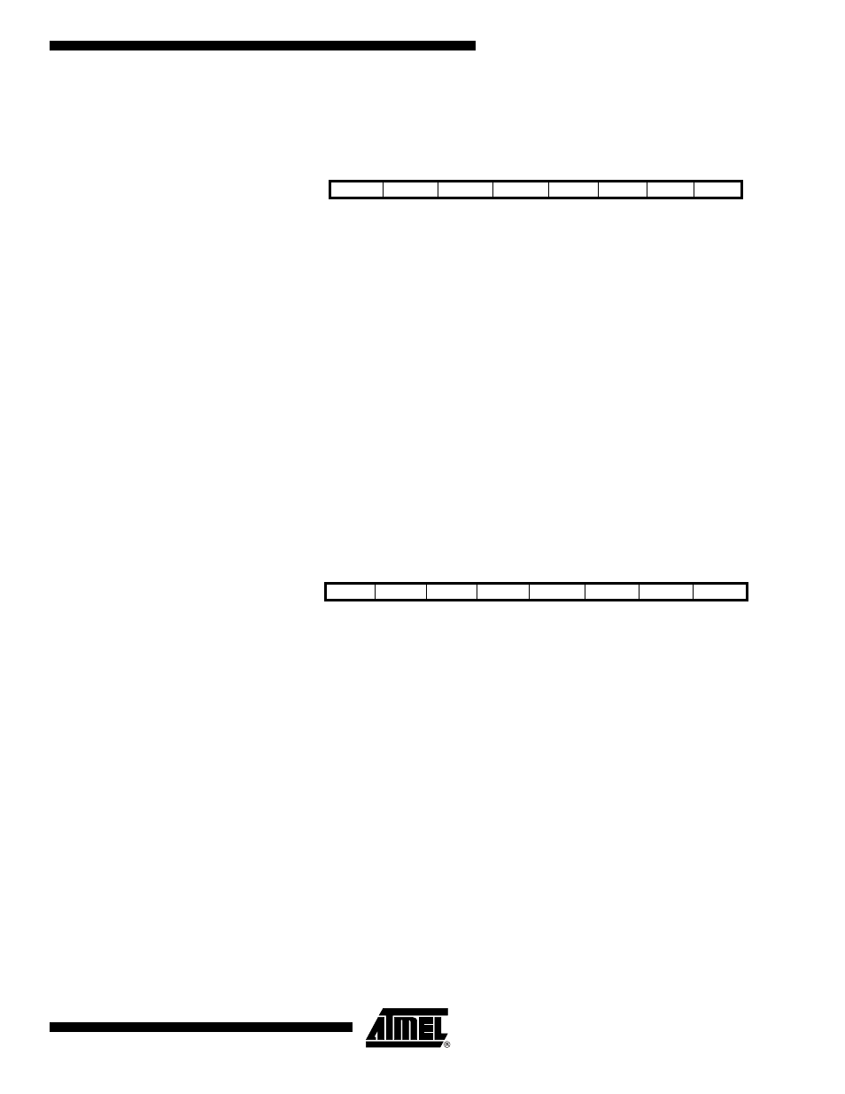
Bit
7
6
5
4
3
2
1
0
MSB
LSB
USIDR
Read/Write
R/W
R/W
R/W
R/W
R/W
R/W
R/W
R/W
Initial Value
0
0
0
0
0
0
0
0
Bit
7
6
5
4
3
2
1
0
USISIF
USIOIF
USIPF
USIDC
USICNT3
USICNT2
USICNT1
USICNT0
USISR
Read/Write
R/W
R/W
R/W
R
R/W
R/W
R/W
R/W
Initial Value
0
0
0
0
0
0
0
0